 +86 755 2794 4155
  sales@knownpcb.com
-
Shenzhen KNOWNPCB Technology Co., Ltd.
 +86 755 2794 4155
  sales@knownpcb.com
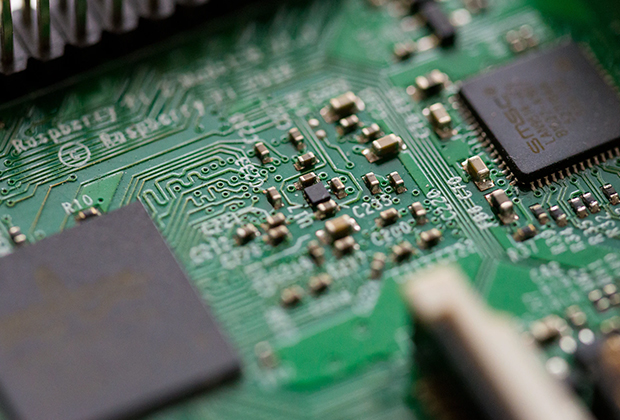
Have you noticed that now more and more of our lighting is using led lighting.What is LED? Compared to the traditional light bulbs, LEDs have lower power consumption, longer lifetime and higher energy efficiency. In the PCB industry,when we say LED PCB, it refers to the pcb used for LED lighting, if you are looking for a suitable LED PCB for your lighting system, this article may bring you something. WHAT ARE LEDS COMPOSED OF?LED is an initial light-emitting diode that produces light when an electric current passes through. LEDs typically have negative and positive electrodes, which generate light in the visible light region.The LEDS are glued to the PCB by soldering process and have electrical connections for lighting.Since light-emitting diodes dissipate a lot of heat when they are in use, when you are designing LED, the metal core is usually the best choice for LED PCB, it is because that it dissipates heat more faster. Among them, the metal material aluminum is the most widely used
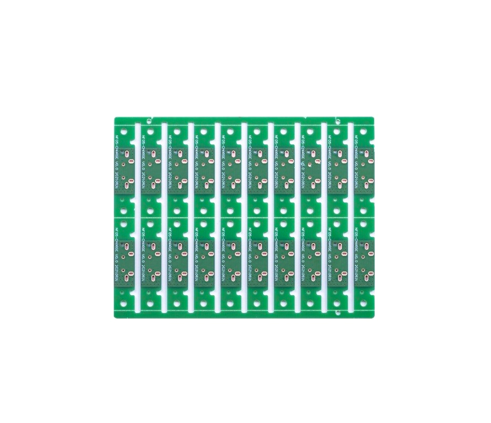
Anime image measuring instrument is applicable to all application fields aiming at two-dimensional measurement, and is widely used in machinery, electronics, instruments, hardware, plastics and other industries. Anime image measuring instrument (also known as image mapping instrument) is based on CCD digital image, relying on computer screen measurement technology and powerful software capabilities of spatial geometry operation. After installing specialized control and graphic measurement software, the computer becomes the measurement brain with the soul of the software and is the main body of the entire device. It can quickly read the displacement value of the optical ruler, and through software module operations based on spatial geometry, instantly obtain the desired results and generate graphics on the screen for the operator to compare the images, thus intuitively distinguishing possible deviations in the measurement results. All of this is done in real-time in front of today
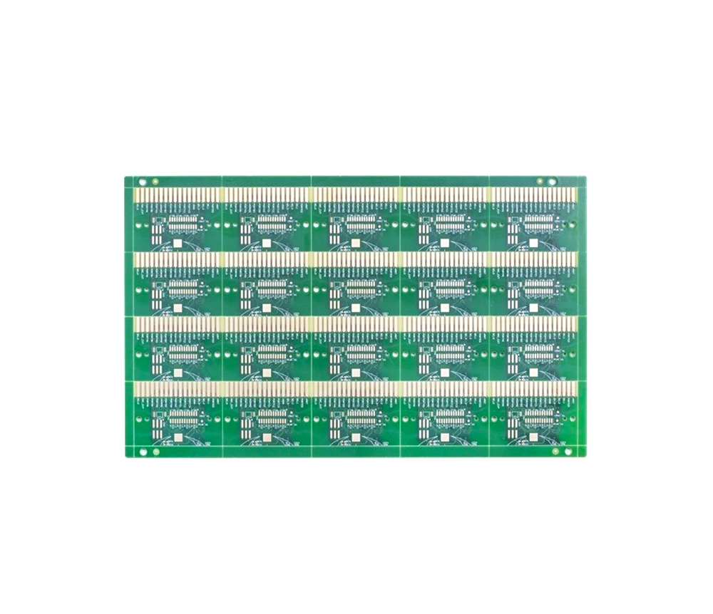
Symptom: There are blasting holes in the cold or solder joints. Inspection method: Conduct regular analysis of the holes before and after immersion welding to identify areas where copper is under stress. In addition, perform incoming inspection on raw materials. Possible reasons: 1. Explosion holes or cold solder joints are seen after soldering operations. In many cases, poor copper plating can lead to expansion during soldering operations, resulting in cavities or explosive holes on the wall of the metallized hole. If this is generated during the wet processing process, the absorbed volatilization The object is covered up by the coating and then driven out under the heating effect of immersion welding, which will create a nozzle or blasting hole. Solution: 1. Try to eliminate copper stress. The expansion of laminates in the z-axis or thickness direction is usually related to the material. It can promote the fracture of metallized pores. Dealing with laminate manufacturers to
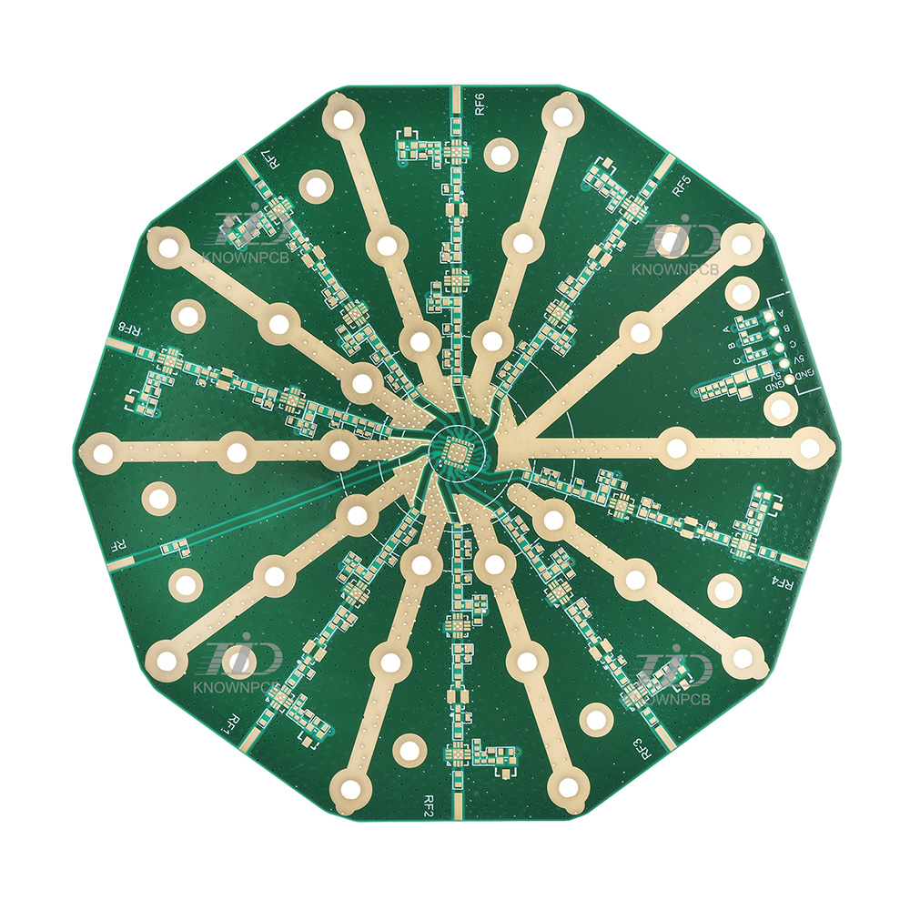
1、 Bridging The causes of bridging are mostly due to excessive solder or severe edge collapse after solder printing, or excessive PCB substrate solder area size, SMD mounting offset, etc. During the refinement stage of SOP and QFP circuits, bridging can cause electrical short circuits and affect product use. 2、 Poor wetting Poor wetting refers to the welding process where the solder and PCB substrate welding area, after being soaked, do not generate metal to metal reactions, resulting in missed or missing solder faults. The reason for this is mostly due to the surface contamination of the welding area, or the adhesion of solder resist, or the formation of a metal compound layer on the surface of the joint, such as the presence of sulfides on the surface of silver and oxides on the surface of tin, which can cause poor wetting. In addition, when the residual aluminum, zinc, cadmium, etc. in the solder exceeds 0.005%, the wetting effect of the solder reduces the activity and can al
Rare metals often need to be plated on board edge connectors, protruding contacts or gold fingers to provide lower contact resistance and higher wear resistance. This technology is called finger plating or protruding part plating. Gold is often plated on the protruding contacts of nickel plated plate edge connectors. The protruding parts of the gold finger or plate edge are manually or automatically plated. Currently, the gold plating on the contact plug or gold finger has been replaced by plating, lead plating, and button plating. The process is as follows: 1) Peel off the coating to remove tin or tin lead coating from protruding contacts 2) Rinse with cleaning water 3) Scrub with abrasive 4) Activated diffusion in 10% sulfuric acid 5) Nickel plating thickness on protruding contacts is 4-5 μ M 6) Cleaning to remove mineral water 7) Gold permeation solution treatment 8) Gilding 9) Cleaning 10) Drying
Whether the quality of PCB ink is excellent or not cannot be separated from the combination of the above major components in principle. Excellent ink quality is the comprehensive embodiment of scientific formula, progressiveness and environmental protection. This is reflected in: Viscosity is the abbreviation for dynamic viscosity. It is generally expressed in viscosity, that is, the shear stress of fluid flow divided by the Velocity gradient in the direction of the flow layer, and the International unit is Pa/s or mPa/s. In PCB production, it refers to the fluidity of ink generated by external forces. Conversion relationship of viscosity units: 1Pa. S=10P=1000mPa. S=1000CP=10dpa. s Plasticity refers to the ability of ink to maintain its pre deformation properties after being deformed by external forces. The plasticity of ink is beneficial for improving printing accuracy; Thixotropy ink is gelatinous when standing, but its viscosity changes when being touched, also known as sh
(1) Heat the waste liquid containing gold to 80-90 ℃, slowly add Iron(II) chloride solution under constant stirring, and the reaction is as follows:; Au3++3Fe2+=3Fe3++Au ↓ As the gold ions are continuously reduced, the color of the solution gradually changes from yellow to crimson, and the gold powder settles at the bottom. Continue to add excess Iron(II) oxide solution and let stand for several hours. Take two drops of static stratification solution and add two drops of 1% red blood salt. The color turns blue, indicating that the gold has been completely reduced. Pour out the upper clear liquid and filter it by vacuum method, while the lower part is precipitated with yellow gold powder. (2) Acid washing and water washing: Add a 1:2.5 hydrochloric acid solution to the gold powder and boil it, stir for 5 minutes, pour out the upper solution, and repeat this process 3-5 times until no yellow color appears. Rinse the gold powder multiple times with distilled water until the pH valu
1、 Unclear definition of processing level The single panel design is on the TOP layer, and if it is not specified, it may be difficult to assemble components on the board without proper explanation. 2、 Large area copper foil too close to the outer frame The distance between the large area copper foil and the outer frame should be at least 0.2mm, as milling onto the copper foil during contour milling can easily cause the copper foil to warp and cause the solder resist to fall off. 3、 Draw solder pads with filler blocks Drawing solder pads with filler blocks can pass DRC inspection during circuit design, but it is not feasible for machining. Therefore, this type of solder pad cannot directly generate solder mask data. When applying solder mask, the filler block area will be covered by solder mask, causing difficulty in device soldering. 4、 The electrical layer is both a solder pad and a connecting wire Because the power supply is designed as a patterned solder pad, the ground
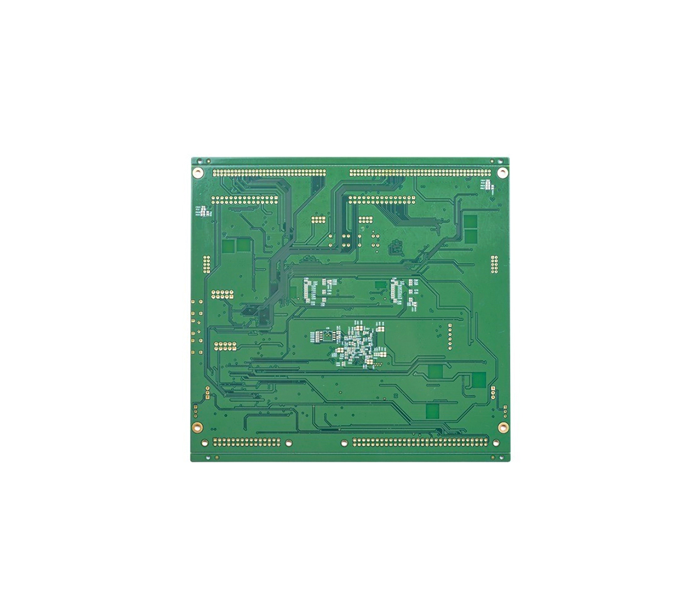
Because there are dozens of types of CAD software popular on the market, the management of CAD processes must be first started from the organization, and good organizations will achieve more effort. Since the GERBER data format has become the standard for the optical painting industry, GERBER data should be processed in the entire optical painting process. If CAD data is used as an object, the following problems will bring. (1) There are too many types of CAD software. If all kinds of process requirements must be completed in CAD software, each operator is required to be proficient in the operation of each CAD software. This will require a long training period to make the operator a skilled worker and meet the actual production requirements. This is not cost -effective from time and economic perspective. (2) Due to the large number of process requirements, some requirements cannot be achieved for certain CAD software. Because CAD software is used for design, it is impossible to m
Inquiry Now

