 +86 755 2794 4155
  sales@knownpcb.com
-
Shenzhen KNOWNPCB Technology Co., Ltd.
 +86 755 2794 4155
  sales@knownpcb.com
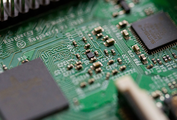
Have you noticed that now more and more of our lighting is using led lighting.What is LED? Compared to the traditional light bulbs, LEDs have lower power consumption, longer lifetime and higher energy efficiency. In the PCB industry,when we say LED PCB, it refers to the pcb used for LED lighting, if you are looking for a suitable LED PCB for your lighting system, this article may bring you something. WHAT ARE LEDS COMPOSED OF?LED is an initial light-emitting diode that produces light when an electric current passes through. LEDs typically have negative and positive electrodes, which generate light in the visible light region.The LEDS are glued to the PCB by soldering process and have electrical connections for lighting.Since light-emitting diodes dissipate a lot of heat when they are in use, when you are designing LED, the metal core is usually the best choice for LED PCB, it is because that it dissipates heat more faster. Among them, the metal material aluminum is the most widely used
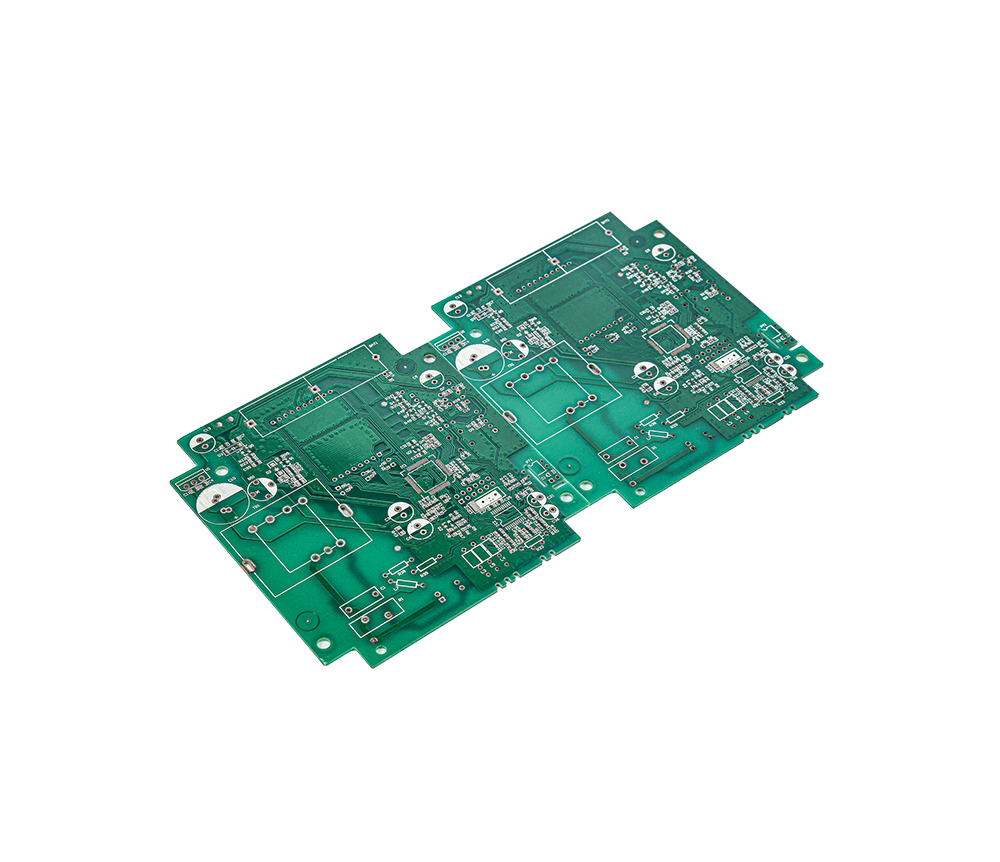
PCB buyers have always been confused about the color of PCB. I don't know what color PCB board is high -quality. Let's explain today what the PCB color affects its performance. First of all, PCB, as a printing line board, mainly provides mutual connection between electronic components. Color and performance are not directly related, and the differences in pigments will not affect electrical. Whether the performance of the PCB board is determined by factors such as the materials used (high Q value), wiring design, and several plates. However, in the process of washing PCB, black is the most likely to cause color difference. If the raw materials and manufacturing processes used by the PCB factory are slightly deviated, the PCB adverse rate will increase due to color difference. This directly leads to an increase in production costs. In fact, the raw materials of PCB are everywhere in our daily life, that is glass fiber and resin. The combination of glass fiber and resin and hardeni
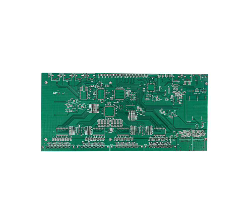
1. Excessive etching of copper foil. The electrolytic copper foil used in the market is generally single -sided galvanized (commonly known as gray foil) and single -sided copper plating (commonly known as red foil). Common copper shampoo is generally galvanized copper above 70um or more Foil, red foil and gray foil below 18um basically have not seen batch -shaped copper. When the customer line design is better than the etching line, if the copper foil specifications change and the etch parameters have not changed, causing the copper foil to stay in the etching solution for too long. Because zinc was originally a lively metal, when the copper line on the PCB was soaked in the etching solution for a long time, it would cause excessive line erosion of the line, resulting in some thin lines against the zinc layer. That is, the copper thread falls off. Another situation is that there is no problem with the PCB etching parameters, but after etching, water washing, and poor drying, result
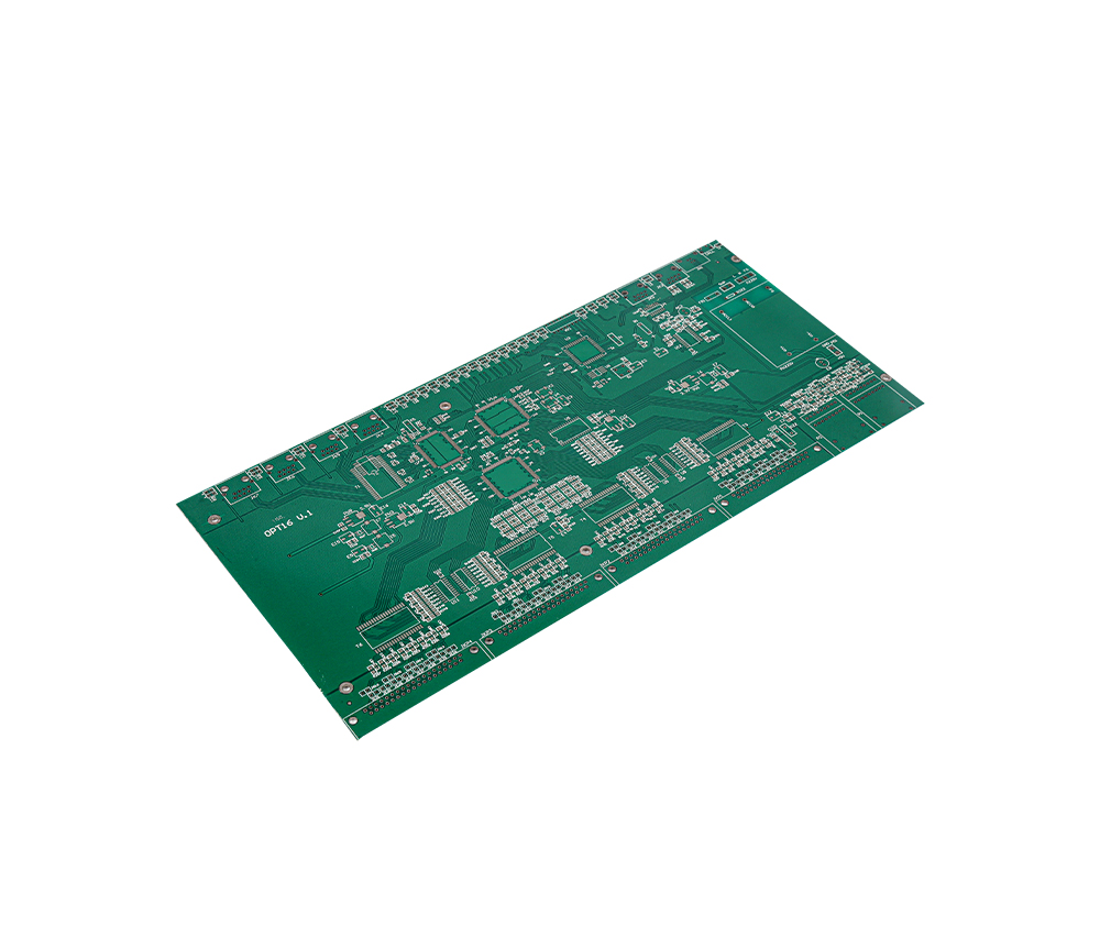
1. It is mentioned that ordinary electrolytic copper foil is a product made by galvan foil or copper plating. The peeling strength is not enough. When the bad foil suppression plate is made into a PCB plug -in in the electronics factory, the copper wire will fall off by the impact of external forces. This type of copper -throwing a copper thread to see the copper foil surface (that is, the contact surface of the substrate). 2. Poor adaptability of copper foil and resin: some special performance layer -made plates used now, such as HTG plates, because the resin system is different, the solid agent is generally PN resin, the resin molecular chain structure is simple, when the solidification is solidified, and when it is solidified The degree of cross -linking is low, and the copper foil with special peak values is necessary to match it. When the production layer is used, the copper foil is not matched with the resin system, resulting in insufficient peeling strength of the plate cov

1. If it is artificial welding, develop good habits. First of all, check the PCB board again before welding, and check whether the key circuits (especially the power supply and land) are used in a multimeter. Test whether the power and land are short -circuited with a multimeter; in addition, do not shake the soldering iron during welding. If you throw the welding to the welding of the chip (especially the table sticker), it is not easy to find it. 2. Open the PCB diagram on the computer, light up the short -circuited network, and see where the closest to see is the most easily connected to one. Pay special attention to the short circuit inside the IC. 3. Find a short circuit. Take a plate to cut the wire (especially suitable for single/double -layer boards), and after cutting the line, each part of the function block is powered on, and part of it is partially excluded. 4. Use short -circuit positioning analyzers, such as: Singapore Proteq CB2000 short -circuit tracking instrume
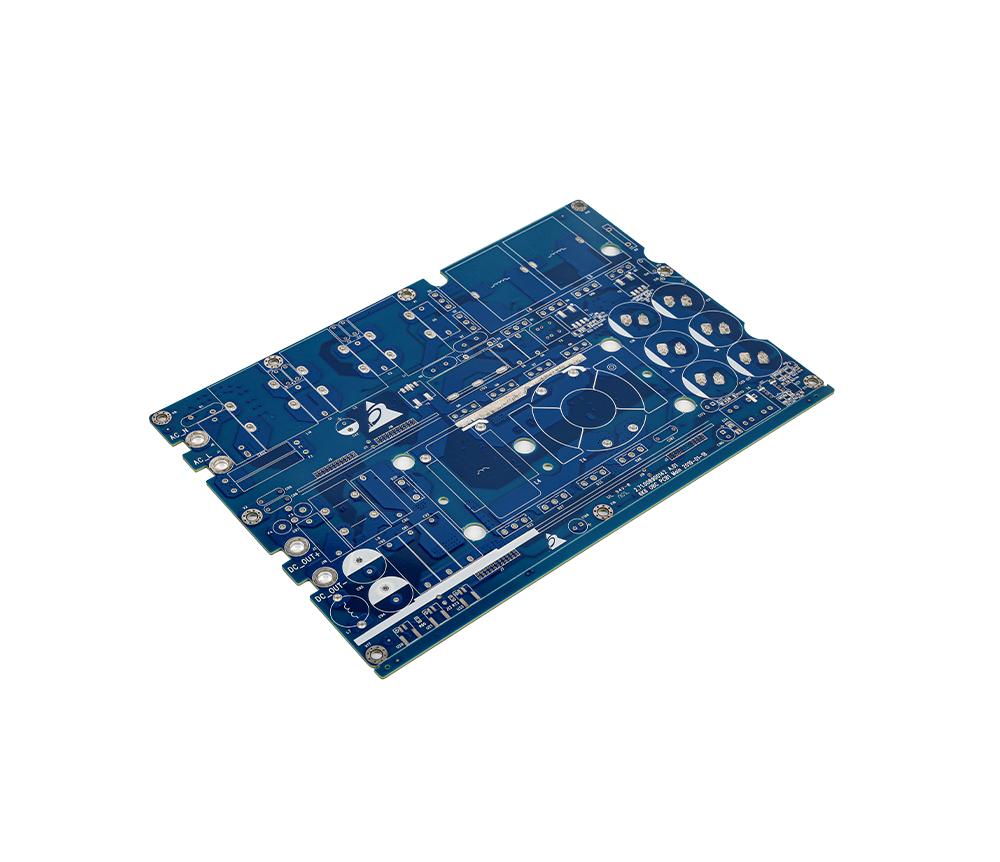
The circuit board includes many types of working levels, such as the signal layer, protective layer, silk printing layer, inner layer, etc. The role of various levels is briefly introduced as follows: ⑴ Signal layer: Mainly used to place components or wiring. Protel DXP usually contains 30 middle layers, namely Mid Layer1 ~ Mid Layer30. The middle layer is used to arrange signal lines, and the top and bottom layers are used to place meta components or copper. Protective layer: It is mainly used to ensure that the tinnic is not required on the circuit board, and it is not plated, thereby ensuring the reliability of the circuit board. Among them, Top Paste and Bottom Paste are top -level welded layers and underlying welded layers; Top Solder and Bottom Solder are the protective layers and underlying tiny paste protective layers, respectively. (3) Silk printing layer: It is mainly used to print the flowing water number, production number, and company name of the component on the ci
The number of layers of the board represents several independent wiring layers. Usually the number of layers is even, and contains two layers on the outermost side. Most of the motherboards are 4 to 8 layers, but it can be technically able to achieve nearly 100 layers of PCB boards. Most of the large supercomputers use quite many layers of motherboards, but because these computers can already replace the cluster of many ordinary computers, the super -multi -layer board has gradually been gradually not used. Because each layer in PCB is closely combined, it is generally not easy to see the actual number, but if you carefully observe the motherboard, you may see. The automatic detection technology of the circuit board is applied with the introduction of surface installation technology, and the packaging density of the circuit board is rapidly increased. Therefore, the automatic detection of the circuit board is not only basic, but also economically even for the low -density and gene
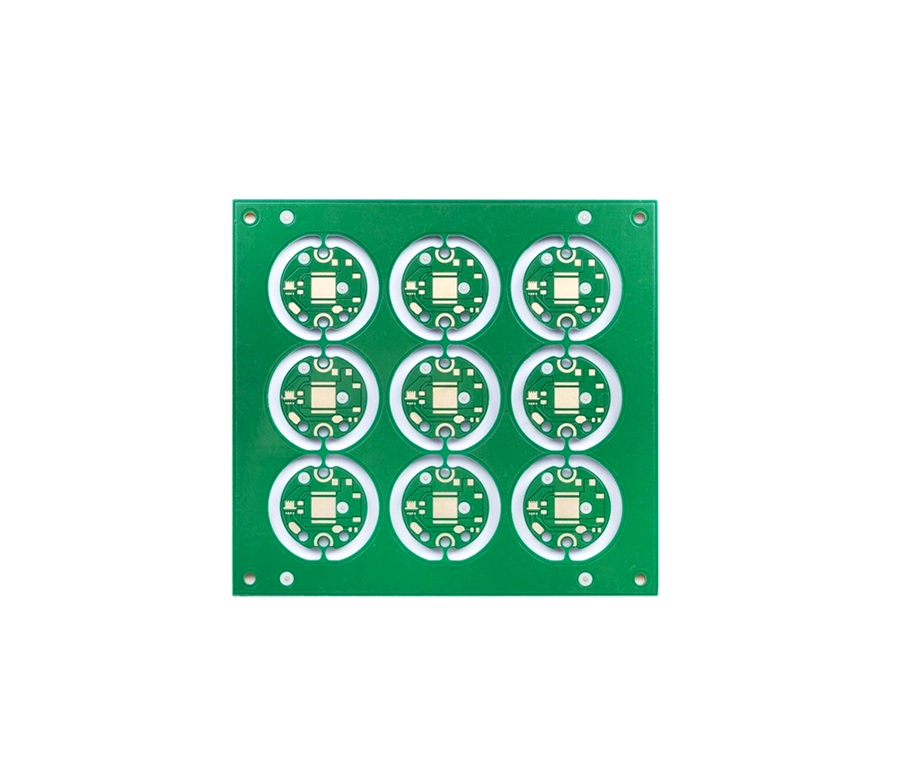
The copper foil substrate is cut into size suitable for processing production. Before the substrate is compressed, it is usually necessary to use brushing, micro -erosion and other methods to properly crudely treat the plate surface of copper foil, and then attach the dry membrane light to the top with appropriate temperature and pressure. Send the substrate with the dry membrane light resistance into the ultraviolet exposure machine to expose. After the light resistance is illuminated by ultraviolet rays in the negative light, it will generate a polymerization reaction (the dry membranes of the area will be in the subsequent development and the copper steps of copper will be will be will be will be will be being being exposed. Keep it as a etching resistant), and move the line image on the negatives to the obstruction of the dry membrane of the plate. After tearing off the protective film on the membrane surface, first use sodium carbonate aquatic solution to remove the zone that
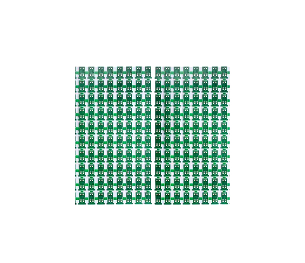
One -panel Single-SIDED BOARDS We just mentioned it, so we call this PCB called Single-SIDED. Because there are many strict limitations on the design lines on the design line (because there is only one side, the path that cannot be handed in the wiring between the wiring is necessary), so only this type of board is used in the early circuit. Double panel Double-size boards There are wiring on both sides of this circuit board. However, to use the wires on both sides, there must be an appropriate circuit connection on both sides. The "bridge" between this circuit is called a guide hole (VIA). The guide hole is a small hole full of metal on PCB, which can be connected to the wires on both sides. Because the area of the double panel is doubled than the single -panel, and because the wiring can be intertwined with each other (it can be around the other side), it is more suitable for more complicated circuits than a single panel. Multi -layer [Multi -layer board] When more complex
Inquiry Now

