 +86 755 2794 4155
  sales@knownpcb.com
-
Shenzhen KNOWNPCB Technology Co., Ltd.
 +86 755 2794 4155
  sales@knownpcb.com
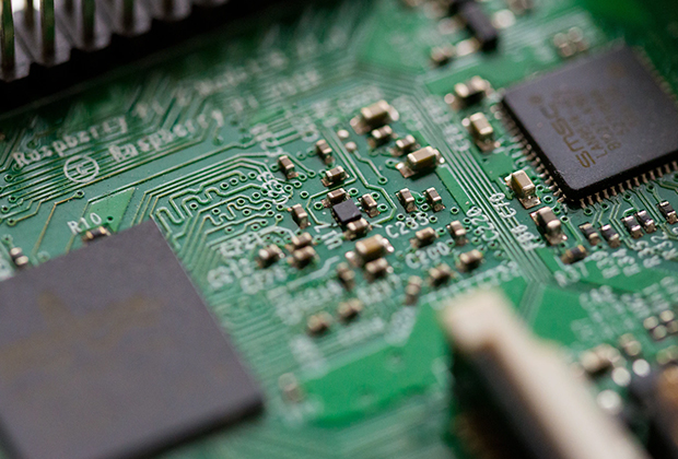
Have you noticed that now more and more of our lighting is using led lighting.What is LED? Compared to the traditional light bulbs, LEDs have lower power consumption, longer lifetime and higher energy efficiency. In the PCB industry,when we say LED PCB, it refers to the pcb used for LED lighting, if you are looking for a suitable LED PCB for your lighting system, this article may bring you something. WHAT ARE LEDS COMPOSED OF?LED is an initial light-emitting diode that produces light when an electric current passes through. LEDs typically have negative and positive electrodes, which generate light in the visible light region.The LEDS are glued to the PCB by soldering process and have electrical connections for lighting.Since light-emitting diodes dissipate a lot of heat when they are in use, when you are designing LED, the metal core is usually the best choice for LED PCB, it is because that it dissipates heat more faster. Among them, the metal material aluminum is the most widely used
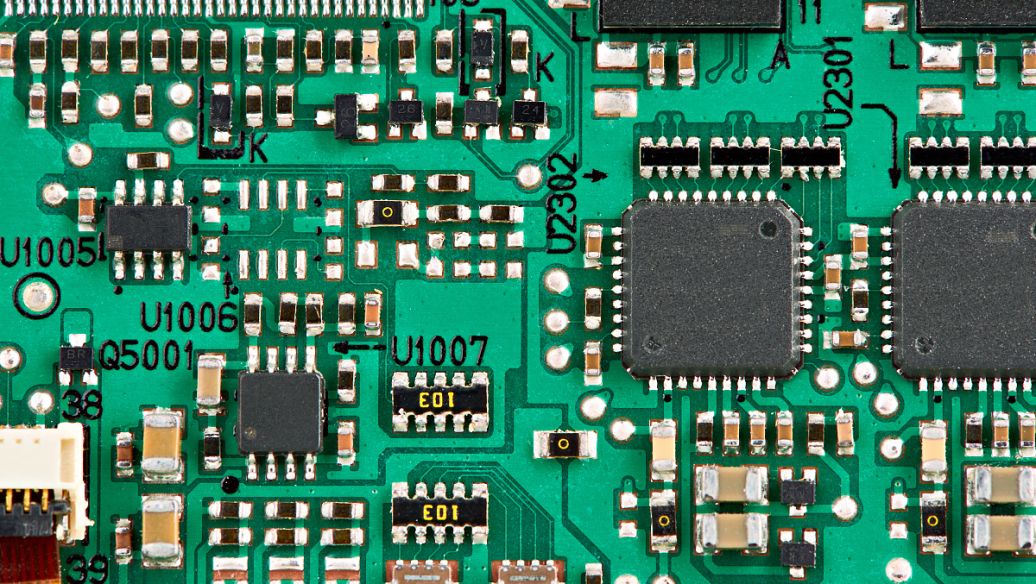
For the design of the chip density and the high clock frequency, the design of the 6 -layer board should be considered. It is recommended to stack the layer: 1. Sig -GND -SIG -PWR -GND -SIG; For this scheme, this superposition layer scheme can get better signal integrity. The impedance of the wiring layer can be better controlled, and both floors can well absorb magnetic lines. And in the case of power and strata, it can provide a good return path for each signal layer. 2. GND -SIG -GND -PWR -SIG -GND; For this solution, this plan is only applicable to the situation where the density density is not very high. This layer has all the advantages of the above layer, and this top and bottom layer The horizon is relatively complete and can be used as a better shield. It should be noted that the power layer should be close to the non -main component surface, because the plane of the bottom layer will be more complete. Therefore, EMI performance is better than the first solution. Summar

For the two -layer board, because the number of plates is small, there is no problem with overlapping layers. Control EMI radiation is mainly considered from wiring and layout; The electromagnetic compatibility of single -layer and double -layer boards is becoming more and more prominent. The main reason for this phenomenon is that the area of the signal circuit is too large, which not only produces strong electromagnetic radiation, but also makes the circuit sensitive to the external interference. To improve the electromagnetic compatibility of the line, the easiest way is to reduce the circuit area of the key signal. Key signals: From the perspective of electromagnetic compatibility, the key signal mainly refers to the signal of strong radiation and a sensitive signal to the outside world. Signals that can generate strong radiation are generally cyclical signals, such as clocks or address low signals. A signal that is sensitive to interference refers to those lower levels of an
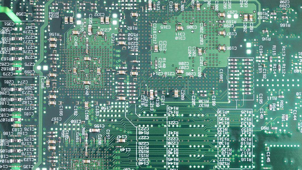
1. SIG -GND (PWR) -PWR (GND) -sig; 2. GND -SIG (PWR) -Sig (PWR) -gnd; For the above two layers of stacking design, the potential problem is the thickness of the traditional 1.6mm (62mil) board. The laminar spacing will become very large, which is not only not conducive to controlling impedance, but also inter -layer coupling and shielding; especially the distance between the power supply formation is very large, reducing the board capacitance, which is not conducive to filtering noise. For the first scheme, there are usually many chips on the board. This scheme can get better SI performance, which is not very good for EMI performance. It is mainly controlled by wiring and other details. Main attention: The connected layer of the signal layer with the most dense signal layer is conducive to absorbing and suppressing radiation; increasing the area of the board and reflecting the 20H rules. For the second scheme, the chip density of the board is usually low enough and there is suff
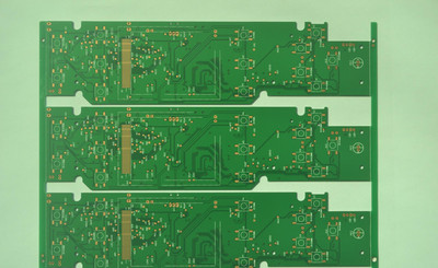
In fact, the four -layer board copy plate is to repeat two double panels, and the sixth floor is to repeat three double panels ... The reason why the multi -layer is daunting is because we cannot see the internal line. How can we see the inner layer of a precise multi -layer board? —— layered. There are many methods on the problem of layered, including potions corroded, knife stripping, etc., but it is easy to divide the layer over the head and lose the information. Experience tells us that sandpaper polishing is the most accurate. When we copy the top layer of the PCB, we usually use sandpaper to polish to grind the surface of the surface to display the inner layer; sandpaper is a common sandpaper sold by the hardware shop. Generally, PCB is paved, then pressing the sandpaper and rubbing on the PCB evenly on the PCB. (If the board is small, you can also lay sandpaper, and press PCB with a finger to rub on the sandpaper). The main point is to pave the flat, so as to grind evenly.
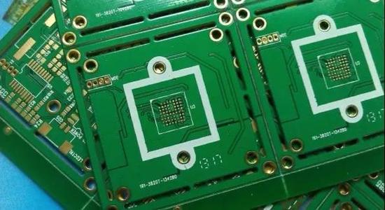
1. Scan the upper and lower surfaces of the circuit board, there are two BMP pictures. 2. Open the copy software QuickPCB2005, click "File" and "Open the bottom diagram" to open a scanning picture. Use Pageup to amplify the screen, see the pad, place a pad in PP, see the line and press PT to walk ... Just like a child drawing, draw it in this software, click "Save" to generate a B2P file. 3. Click the "File" and "Open the bottom diagram" to open another layer of scanning color map; 4. Click the "File" and "Open" to open the B2P file saved in front. We see the just copied board and stacked on this picture -the same PCB board, the hole is in the same position, but the line connection is different from different line connections. Essence Therefore, we according to the "Options" - "layer settings", here to turn off the displayed lines and silk prints, leaving only a multi -layer perforated. 5. The excessive hole on the top layer is in the same position as the perforated on the bott
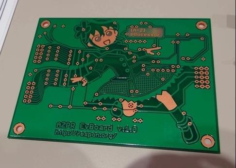
In simple terms, it is to scan the circuit board to be copied first, record the detailed component location, and then remove the component to make it into a material list (BOM) and arrange the material procurement. Treatment to the PCB board diagram file, and then send the PCB file to the production plate. After the board is made, the purchased components are welded to the PCB board made, and then the circuit board can be tested and debugged. The specific technical steps are as follows: The first step is to get a PCB. First, record the models, parameters, and positions of all components on the paper on the paper. It is best to take a picture of two component positions with a digital camera. Many PCB circuit boards, the more advanced the diodes, the two pole trigelines, are not paid to see. The second step is to remove all devices and remove the tin in the PAD hole. Wash the PCB with alcohol, and then put it in the scanner. When scanning, you need to adjust the pixels of the scan
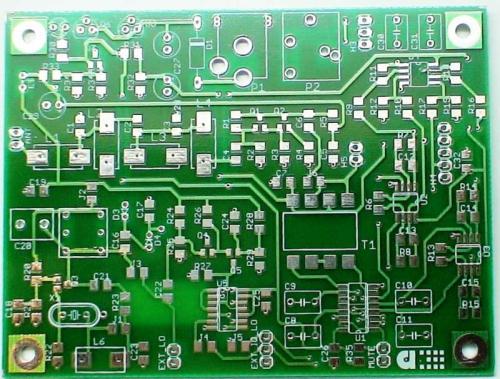
The PCB copy is a category of reverse engineering. Since the birth of the entire concept, it has been under extensive controversy. The method of reverse engineering has played a huge role in the development of the integrated circuit industry. Methods to understand the development of other people's products. If this behavior is strictly prohibited, it will affect the advancement of integrated circuit technology. Therefore, countries will be regarded as an exception of infringement under certain conditions when legislative. In order to teach, analyze and evaluate the concepts, technology, or the circuit, logical structure, and component configuration used in the design of the cloth design, copy the cloth design and apply the analysis and evaluation results to the original cloth map on this basis In the design, the integrated circuit is made based on this, which is not regarded as infringement. However, it should be considered as infringement, which simply replicate the protection of

Many people have misunderstandings about the concept of PCB copy plate. In fact, with the continuous development and deepening of the copy of the board industry, today’s PCB copy concept has been extended widely, and it is no longer limited to the copy and cloning of simple circuit boards and cloning. It will also involve the second development of the product and the development of new products. For example, through the analysis of existing product technical documents, design ideas, structural characteristics, process technology, etc., you can provide feasibility analysis and competitive reference for the research and development and design of new products, and assist R & D design units to follow up the latest. The technological development trend, timely adjust the improvement of product design plans, and develop the most competitive new products in the market. At the same time, the process of PCB copy plate through the extraction and partial modification of the technical data file
Inquiry Now

