 +86 755 2794 4155
  sales@knownpcb.com
-
Shenzhen KNOWNPCB Technology Co., Ltd.
 +86 755 2794 4155
  sales@knownpcb.com
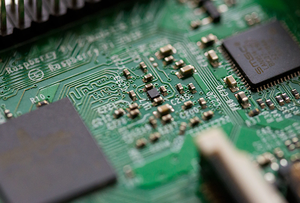
Have you noticed that now more and more of our lighting is using led lighting.What is LED? Compared to the traditional light bulbs, LEDs have lower power consumption, longer lifetime and higher energy efficiency. In the PCB industry,when we say LED PCB, it refers to the pcb used for LED lighting, if you are looking for a suitable LED PCB for your lighting system, this article may bring you something. WHAT ARE LEDS COMPOSED OF?LED is an initial light-emitting diode that produces light when an electric current passes through. LEDs typically have negative and positive electrodes, which generate light in the visible light region.The LEDS are glued to the PCB by soldering process and have electrical connections for lighting.Since light-emitting diodes dissipate a lot of heat when they are in use, when you are designing LED, the metal core is usually the best choice for LED PCB, it is because that it dissipates heat more faster. Among them, the metal material aluminum is the most widely used
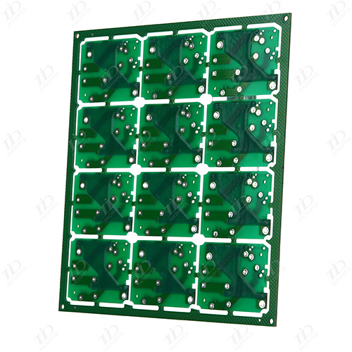
As an important part of the PCB design, whether it is domestic PCB design software or some protes abroad, PowerPCB provides intelligence, so how can I apply the copper. Swinging brings benefits. The so -called copper covering is to use the idle space on the PCB as the benchmark surface, and then fill it with solid copper. These copper areas are also called irrigated copper. The significance of copper covering is to reduce the impedance of the ground and improve the anti -interference ability; reduce the pressure drop and improve the efficiency of the power; connect with the ground line, and can also reduce the area of the circuit. In order to allow PCB to welded as much as possible, most PCB manufacturers also require PCB designers to fill the copper skin or grid -like ground line in the empty area of PCB. If the copper covering is not handled properly, it will be worthless. Is the copper covering "benefits greater than the disadvantages" or "disadvantage is greater than benefits
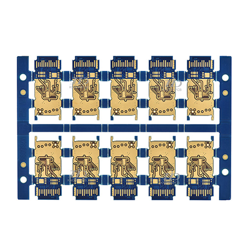
1. If there are many land in PCB, there are SGND, Agnd, GND, etc., and according to the different positions of the PCB board surface, you should use the main "ground" as the benchmark reference to cover the copper. Digital ground and simulation are separated to cover copper. Before the copper is covered, the corresponding power connection is first thicken: 5.0V, 3.3V, etc. In this way structure. 2. For single -point connections in different places, the method is to connect through 0 Euro resistance, magnetic beads or inductance; 3. Copper crop near the crystal, the crystal in the circuit is a high -frequency transmission source, the method is to surround the crystal correction copper, and then the crystal shell is grounded separately. 4. If the island (dead area) problem, if it feels very large, it will not take much money to define a place to add the holes. 5. When starting the wiring, deal with the ground wires, and you should take the ground wire well when you walk. You cann
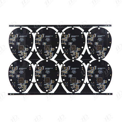
(1) The ERC reports have no access signal: a. Define the I/O attributes for the pipeline when creating packaging; b. Modify the inconsistent GRID attributes when creating an element or placing an element. c. When creating components, the direction of PIN is reverse, and it must be unconnected in the PIN NAME end. d. The more common reasons are that there are no engineering documents. This is a mistake that beginners make. (2) Components run outside the drawing industry: No components are created in the component library diagram table paper center. (3) The created engineering file network table can only be partially transferred to the PCB: when generating Netlist, no selection is Global. (4) When using multiple parts created by yourself, do not use Annotate.
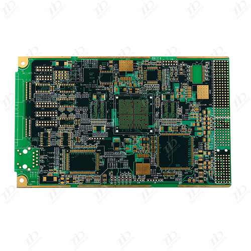
(1) Report node when the network is loaded, not found a. The components in the schematic diagram use the package that is not available in the PCB library; b. The components in the schematic diagram use the name of the name in the PCB library inconsistently packaging; c. The components in the schematic diagram use the PIN Number in the PCB library inconsistent packaging. For example, the triode: Pin Number in SCH is E, B, C, and PCB is 1, 2, 3. (2) You can never print it on a page when printing a. No at the original point when creating the PCB library; b. Move and rotate components multiple times, and there are hidden characters outside the PCB board. Select all hidden characters, reduce PCB, and then move the character to the boundary. (3) The DRC report network is divided into several parts: It means that this network is not connected, read the report file, and select the Connected Copper to find. If it is more complicated, try not to use automatic wiring.
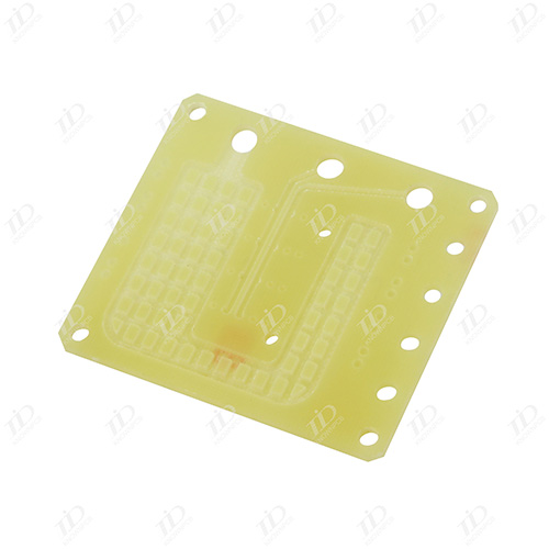
1. Engineering Design The arrangement of interlayer semi cured sheets should correspond; Multi layer core boards and semi cured sheets should use the same supplier's products; The outer C/S surface graphics area should be as close as possible, and independent grids can be used; 2. Drying board before cutting Generally, at 150 degrees Celsius for 6-10 hours, the moisture inside the board is removed, further allowing the resin to cure completely and eliminating stress inside the board; Drying the board before opening, both the inner layer and both sides are required! 3. Attention should be paid to the warp and weft directions of the cured sheet before laminating the multi-layer board The shrinkage ratio in the warp and weft directions is different, so pay attention to distinguishing the warp and weft directions before cutting and stacking the semi cured sheet; When cutting the core board, attention should also be paid to the warp and weft directions; The general direction of the
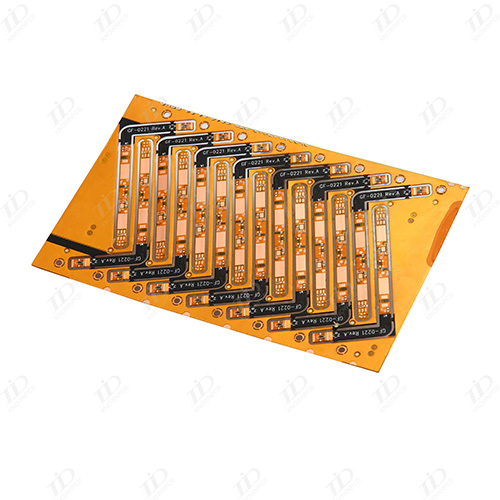
Poor solderability of circuit board holes will result in solder defects, affecting the parameters of components in the circuit, leading to unstable conduction of multi-layer board components and inner wires, and causing the entire circuit function to fail. The so-called weldability refers to the property of the metal surface being wetted by molten solder, which means that the solder forms a relatively uniform and continuous smooth adhesive film on the metal surface. The main factors affecting the solderability of printed circuit boards are: (1) the composition of the solder and the properties of the soldered material. Solder is an important part of the welding chemical treatment process. It consists of chemical materials containing flux. The commonly used low melting point eutectic metal is Sn Pb or Sn Pb Ag. The impurity content should be controlled in proportion to prevent the oxide produced by impurities from being dissolved by flux. The function of solder is to help wet the sur
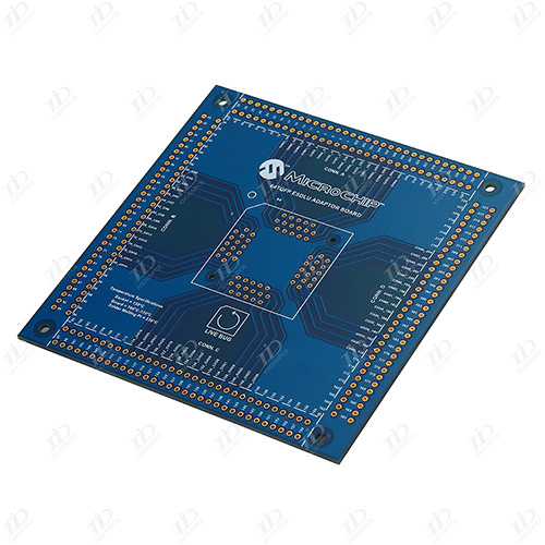
In terms of layout, when the circuit board size is too large, although welding is easier to control, the printed lines are longer, the impedance increases, the noise resistance decreases, and the cost increases; Over time, the heat dissipation decreases, making it difficult to control welding and prone to interference between adjacent lines, such as electromagnetic interference from circuit boards. Therefore, it is necessary to optimize PCB board design: (1) shorten the wiring between high-frequency components and reduce EMI interference. (2) Components with large weight (such as exceeding 20g) should be fixed with brackets and then welded. (3) Heating elements should consider heat dissipation to prevent significant surface damage Δ If defects occur and rework occurs, the thermistor should be kept away from the heat source. (4) The arrangement of components should be as parallel as possible, which is not only aesthetically pleasing but also easy to weld, making it suitable for mass
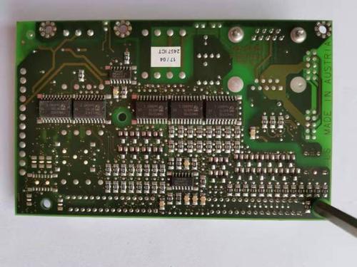
Firstly, during the production and processing of PCB boards, there will be a certain proportion of defective products. At this point, we need to use mechanical equipment to inspect and screen out unqualified defective products. Therefore, we need to conduct electrical testing. So, what is the difference between testing and flying needle testing? The testing is divided into test fixture testing and flying needle testing, In terms of speed, the test frame test will be faster, and the flying needle test will be slower In terms of cost, the cost of testing racks is higher As for which testing method to choose, we need to choose based on the number of PCBs. For those with a large number, choose a testing rack, and for those with a small number, choose flying pins Based on cost, time efficiency, and comprehensive evaluation and selection
Inquiry Now

