 +86 755 2794 4155
  sales@knownpcb.com
-
Shenzhen KNOWNPCB Technology Co., Ltd.
 +86 755 2794 4155
  sales@knownpcb.com
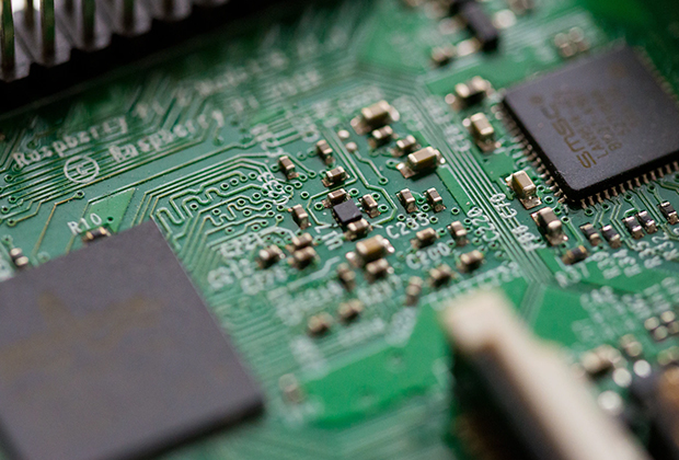
Have you noticed that now more and more of our lighting is using led lighting.What is LED? Compared to the traditional light bulbs, LEDs have lower power consumption, longer lifetime and higher energy efficiency. In the PCB industry,when we say LED PCB, it refers to the pcb used for LED lighting, if you are looking for a suitable LED PCB for your lighting system, this article may bring you something. WHAT ARE LEDS COMPOSED OF?LED is an initial light-emitting diode that produces light when an electric current passes through. LEDs typically have negative and positive electrodes, which generate light in the visible light region.The LEDS are glued to the PCB by soldering process and have electrical connections for lighting.Since light-emitting diodes dissipate a lot of heat when they are in use, when you are designing LED, the metal core is usually the best choice for LED PCB, it is because that it dissipates heat more faster. Among them, the metal material aluminum is the most widely used
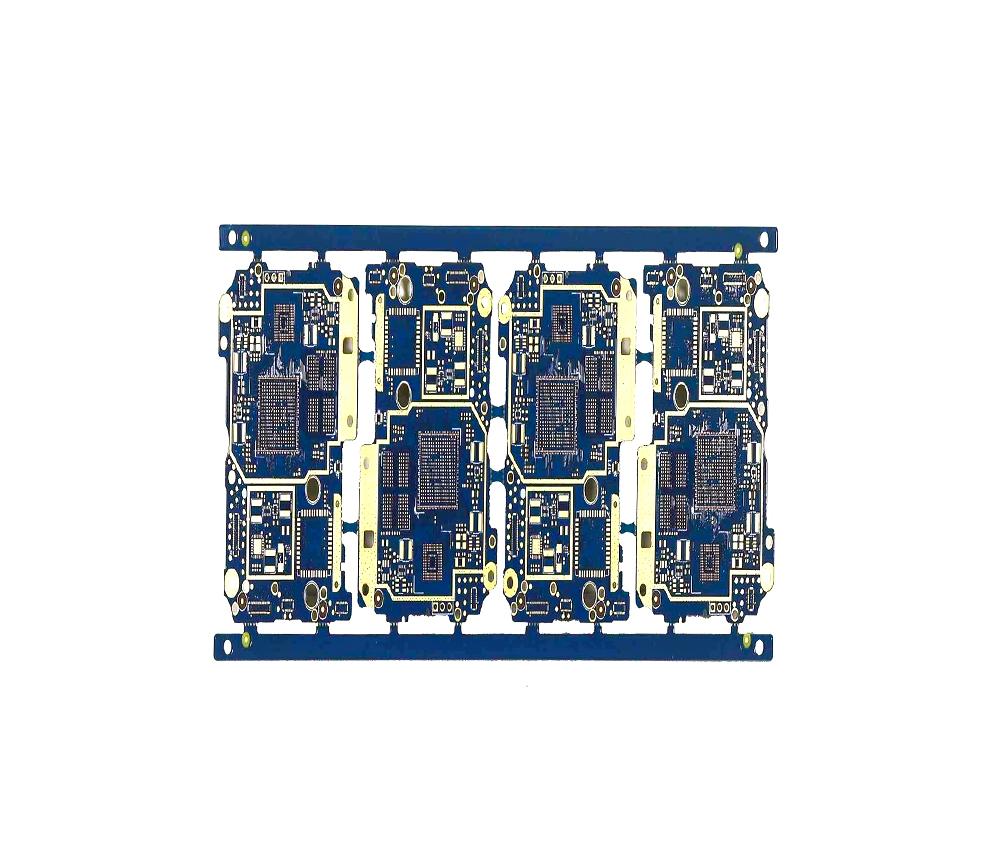
This method is connected to each detection point on the circuit board from a probe with a spring. The spring makes each probe with 100 -200g pressure to ensure that each detection point is well -touched. Such a probe is called "needle bed" together. Under the control of the detection software, the detection point and the detection signal can be programmed. Figure 14-3 is a typical needle bed tester structure. Detectors can know the information of all test points. In fact, only the probes of test points that need to be tested are installed. Although the needle bed test method may be detected at both sides of the circuit board at the same time. When designing the circuit board, all the detection points should still be on the welding surface of the circuit board. Needle tester equipment is expensive and difficult to repair. The needle selects different arrangements according to its specific application. A basic general raster processor is composed of a drilling board with a pitch of
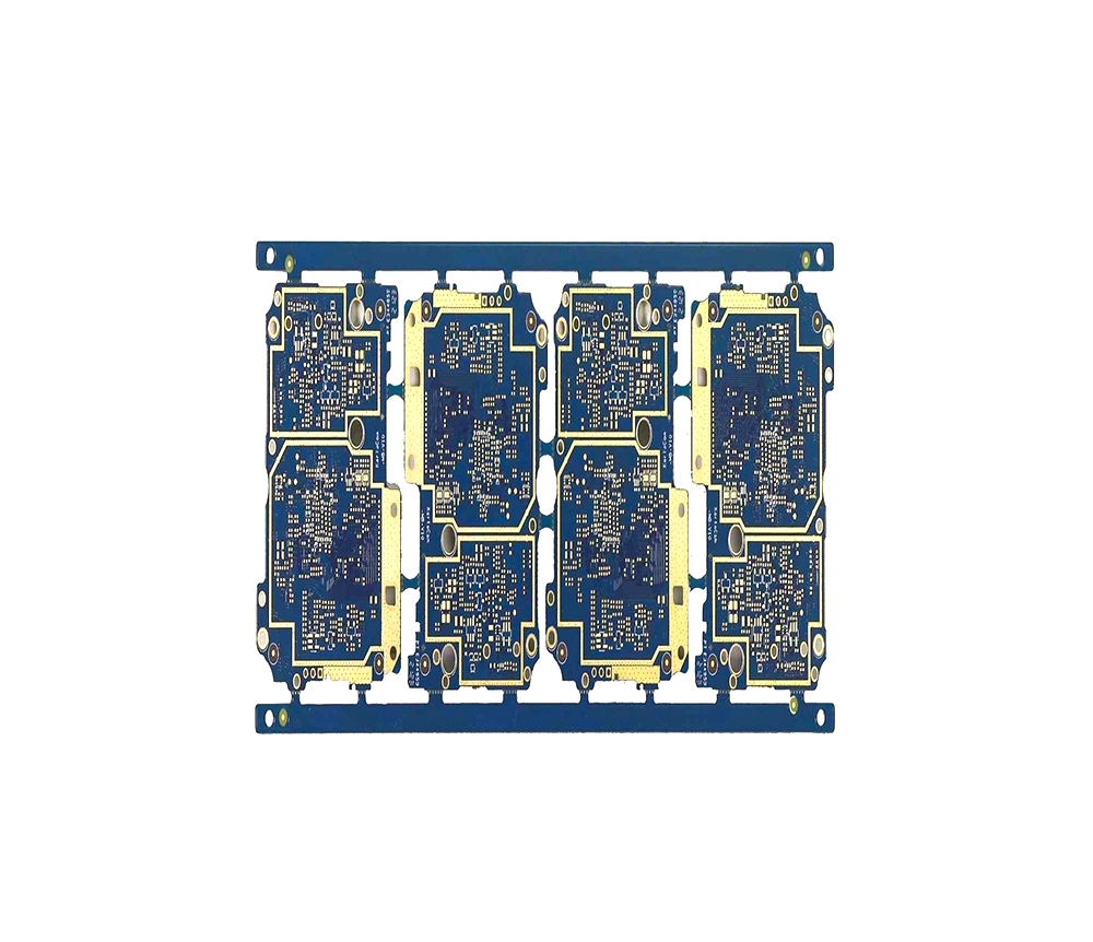
1. OSP main component concentration: alkyl pyramazole or similar ingredients (imazole) is the main ingredient in OSP medicinal solution. The concentration of the concentration is the root of determining the thickness of the OSP membrane. 2. Organic acid: The addition of organic acid can increase the solubility of alkyl pyramazole in the aqueous solution. Promote the formation of a combination of protective film. However, too much dosage can dissolve the protective membrane deposited on the surface of the copper, so it is crucial to control the added value of organic acid (ie, the pH value). When the pH value is too high, the solubility of the alkyl pyramole is reduced, and the oil -shaped object is precipitated, which is not good for immersion. The pH value control can obtain a complex with a dense, uniform, and thick thickness. When the pH value is too low, the solubility of the linked membrane increases, which can dissolve the complex deposited on the copper without forming a me
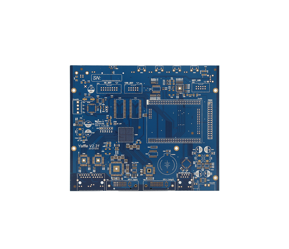
Causes of tin beard: 1. The mutual diffusion between the tin and the copper forms metal interoperability, resulting in the rapid growth of the internal pressure stress of the tin layer, resulting in the diffusion of the tin atom along the crystal boundary to form tin beard; 2. The residual stress of the plating layer after electroplating causes the growth of tin beards. solution: 1. Electro -plating fog tin, change the structure of its crystals, and reduce stress; 2. Bake up at 150 for 2 hours. (Experiments have proved that at more than 90, tin beard will stop growing) 3. Add a small amount of organic metal additives for ENTHONE FST ingening process to limit the raw of tin copper metal interoperabilitybecome; 4. Add a layer of blocking layer between tin and copper, such as nickel layer.
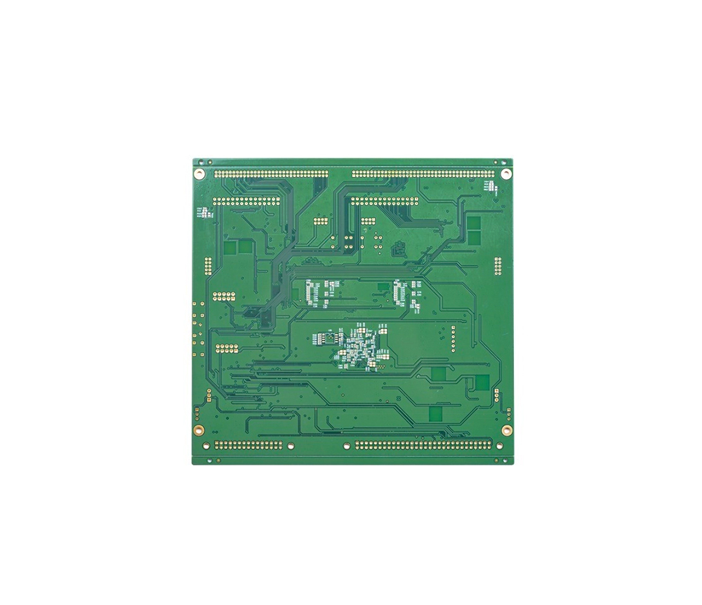
Circuit board short circuits are a problem that almost every circuit board manufacturer encounters on a daily basis, and such problems have always troubled production and quality management personnel. The problems caused by it include replenishment due to insufficient shipment quantity, delayed delivery, and customer complaints, which are relatively difficult for industry insiders to solve. We first summarize and classify the main causes of PCB open circuits into the following aspects: Open circuit caused by exposed substrate: 1. There are scratches on the copper clad plate before entering the warehouse; 2. The copper clad plate was scratched during the cutting process; 3. The copper clad plate was scratched by the drilling nozzle during drilling; 4. The copper clad plate was scratched during transportation; 5. The surface copper foil was damaged due to improper operation during the stacking of boards after copper deposition; 6. The copper foil on the surface of the product
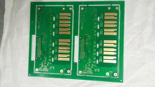
1. Before entering the warehouse, IQC must conduct spot checks on the copper clad board to check if there are any scratches or exposed substrate on the board surface. If there are any, the supplier should be contacted in a timely manner and appropriate measures should be taken based on the actual situation. 2. The copper clad plate was scratched during the cutting process, mainly due to the presence of hard and sharp objects on the cutting machine table. During the cutting process, the copper foil was scratched and the substrate was exposed due to friction between the copper clad plate and the sharp objects. Therefore, before cutting, the table must be carefully cleaned to ensure that the table is smooth and free of hard and sharp objects. 3. The copper clad plate was scratched by the drill bit during drilling, mainly due to the wear of the spindle clamp or the uncleaned debris inside the clamp. The PCB sampling grab drill bit cannot grip firmly, and the drill bit does not reach
The advantages and disadvantages are obvious: Advantages: Low cost, flat surface, good weldability (without oxidation). Disadvantages: It is easily affected by acid and humidity and cannot be stored for a long time. It needs to be used up within 2 hours after opening the seal, as copper is prone to oxidation when exposed to air; It cannot be used on double-sided boards because the second side has already oxidized after the first reflow soldering. If there is a Test point, solder paste must be printed to prevent oxidation, otherwise it will not be able to contact the probe well later. Pure copper is easily oxidized when exposed to air, and the outer layer must have the above protective layer. And some people believe that the golden color is copper, which is a wrong idea because it is the protective layer on top of copper. So it is necessary to extensively gild the circuit board, which is the gold deposition process that I have previously introduced to everyone.
Gold is the true gold. Even if only a very thin layer is plated, it already accounts for nearly 10% of the cost of the circuit board. There are many merchants in Shenzhen who specialize in purchasing waste circuit boards and use certain means to wash out gold, which is a good income. The use of gold as a coating is for the convenience of welding and for corrosion prevention. Even the gold fingers of memory modules that have been in use for several years still flicker like before. If copper, aluminum, and iron were used in the past, they would now rust into a pile of waste. The gold plating layer is widely used in the solder pads, gold fingers, connector shrapnel and other positions of circuit boards. If you find that the circuit board is actually silver, it goes without saying. If you directly call the consumer rights hotline, it must be that the manufacturer cut corners, did not use the materials properly, and used other metals to deceive customers. The motherboards of the most
As a manufacturer, you know that the quality of products depends on the components you use. When it comes to printed circuit boards (PCBs), the color of the board may not seem important,but have you ever wondered if the color of a PCB board can determine its quality? The raw material of pcb is everywhere in our daily life, that is, glass fiber and resin, glass fiber and resin combined, hardened, became a kind of heat insulation, insulation, and not easy to bend the board, this is the pcb substrate, of course, light by the combination of glass fiber and resin pcb substrate can not be transmitted to the signal, so on the pcb substrate, The manufacturer will cover the surface with a layer of copper, so the pcb substrate can also be called a copper-coated substrate The color of a PCB board has no direct correlation with its performance. The performance of a PCB board is determined by the materials used, wiring design, and number of layers. However, during the PCB washing process, bla
Inquiry Now

