 +86 755 2794 4155
  sales@knownpcb.com
-
Shenzhen KNOWNPCB Technology Co., Ltd.
 +86 755 2794 4155
  sales@knownpcb.com
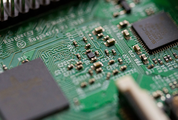
Have you noticed that now more and more of our lighting is using led lighting.What is LED? Compared to the traditional light bulbs, LEDs have lower power consumption, longer lifetime and higher energy efficiency. In the PCB industry,when we say LED PCB, it refers to the pcb used for LED lighting, if you are looking for a suitable LED PCB for your lighting system, this article may bring you something. WHAT ARE LEDS COMPOSED OF?LED is an initial light-emitting diode that produces light when an electric current passes through. LEDs typically have negative and positive electrodes, which generate light in the visible light region.The LEDS are glued to the PCB by soldering process and have electrical connections for lighting.Since light-emitting diodes dissipate a lot of heat when they are in use, when you are designing LED, the metal core is usually the best choice for LED PCB, it is because that it dissipates heat more faster. Among them, the metal material aluminum is the most widely used
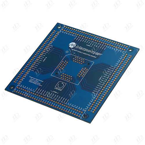
1 process process The printed board of the graphic plate → acid oil removal → scanning water washing → secondary countercurrent water washing → micro -erosion → scanning water washing → secondary countercurrent water washing → copper plating pre -immersing → copper plating → scanning water washing → pre -immersion of tin plating → Tin -plated → III countercurrent water washing → lower panel 2 Detailed process process 2.1 Tin -plated pre -immersion 2.1.1 Composition and operating conditions of tin -plated pre -immersion fluid 2.1.2 The cylinder method of pre -immersing tin -plated groove Add half -cylinder distilled water first, then slowly immerse the 15L mass score of 98%, stir and cool down, add 1.5L Sulfotech Part A, stir well, add distilled water to 300L and stir well to use it. 2.1.3 The maintenance and control of tin -plated pre -immersed groove liquid Each treatment of 100m2 plates requires 1L sulfuric acid and 100mlsulfotech part A. Whenever the slot is treated with
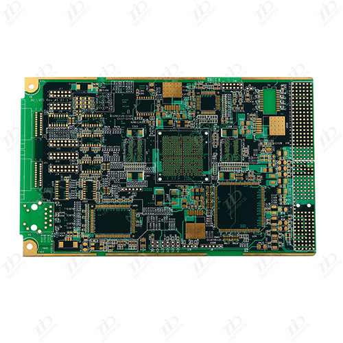
High -speed PCB design rules are usually divided into two types: physical rules and electrical rules. The so -called physical rules refer to some design rules based on physical dimensions. For example, the line width is 4mi1, the distance between the line is 4mi1, and the length of the parallel wiring is 4mi1. The electrical rule refers to the design rules related to electrical characteristics or electrical performance, such as wiring delay control between INS and 2NS, and the total amount of stringing on a certain PCB line is less than 70mV. Define the physical rules and electrical rules to further explore high -speed wiring. High -speed wirms based on physical rules (physical rules) include AutoActive RENers, CCT wiring, B1AZEROUTER wiring, and Router Editor wiring. In fact, these wiringers are automatic wiring drivers of physical rules, which is It is said that these roders can only automatically meet the requirements of the physical dimensions specified by the design engineer,

Digital systems have strict requirements for timing. In order to meet the requirements of the signal timing, adjustment of the signal wiring on the PCB has become part of the PCB design work. Adjusting the wiring length includes two aspects: relative and absolute. The so -called relative is that the length of the wiring is consistent, and ensure that the signal is synchronized to several receivers. Sometimes there is correlation between a set of signal lines on PCB. For example, the bus needs to be corrected, because the signal needs to be synchronized at the receiving end. Its adjustment method is to find out the longest wiring, and then adjust other wiring to the equal length. The absolute requirement is to control the delay of the wiring between the two devices to a certain value, such as the delay between the device A and B as the ins, and this requirement is often proposed by the high -speed circuit designer, and the PCB engineer will realize it. Essence To meet this require
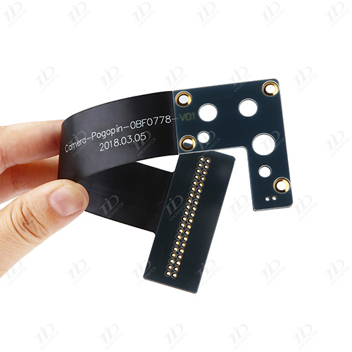
PCB multi -layer board refers to the multi -layer line board used in electrical products. The multi -layer board uses more single -panel or double panel wiring board. Use one double -sided as the inner layer, two -sided single -sided as the outer layer or two double -sides as the inner layer, two -sided single -sided outer layer printing line board, alternate the positioning system and insulating bonding material, and the electrophoretic graphics The interconnected printing circuit boards are made according to design requirements. With the continuous development of SMT (surface installation technology) and the continuous launch of the new generation of SMD (surface installation device), such as QFP, QFN, CSP, BGA (especially MBGA), make electronic products more intelligent and miniaturized, so Promote major reforms and progress of PCB industry technology. Since IBM first successfully developed high -density and multi -layer boards (SLC) in 1991, major groups from various countries
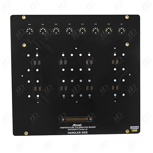
Since the mid -1980s in the mid -1980s, its output value and production have increased at a rate of more than 10 % (compared with the previous year). Because the components develop rapidly to `light, thin, short, small" " Multi -layer boards will be the most influential and vitality door category in the printing circuit board industry, and become the leading product. The multi -layer plate structure will move towards diversified and thin -level high -level, while the M C m one L structure will be faster faster. Development. Multi -layer board requires high device and technology investment. In the future, high -level multi -layer boards will be concentrated in strong PC B large manufacturers to develop and produce High density Thin, high (high) layered Diversity of multi -layer plate structures The thin substrate of the high -performance thin copper box High flatness and surface coating technology of the board surface Dead multi -layer board and rigidity multi -layer board
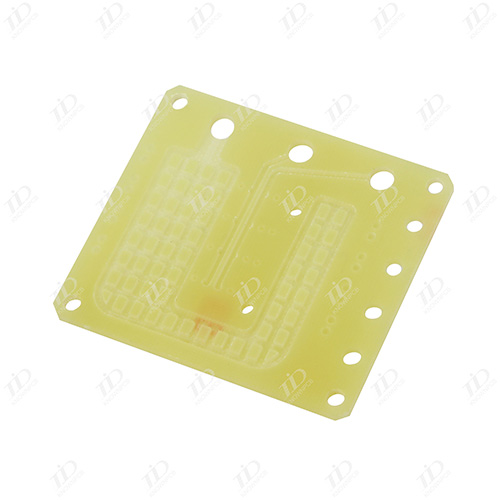
Any printing board has the problem of assembly with other structural parts. Therefore, the shape and size of the printed board must be based on the structure of the product [5]. However, from the perspective of production technology, it should be as simple as possible. Generally, it is a rectangular shape that is not very different in length and width to facilitate assembly, improve production efficiency, and reduce labor costs. In terms of number of layers, it must be determined according to the requirements of the circuit performance, the size of the board, and the density of the circuit. For multi -layer printing boards, the application of four -layer board and six -layer board is the most widely used. Taking four layers of boards as an example, the two wire layers (component surface and welding surface), a power layer, and a formation. Each layer of the multi -layer board should be symmetrical, and it is best to count the bronze layer, that is, four, six, and eight layers. Be
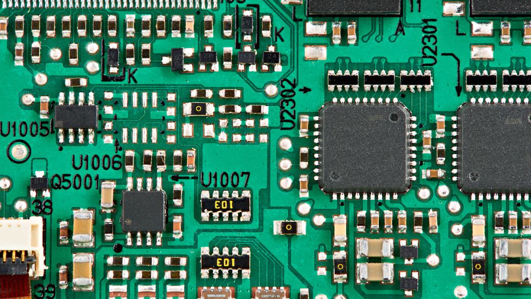
1. The MeChanical mechanical layer, as its name implies, is used for mechanical molding, that is, the appearance of the entire PCB. In fact, when we talk about the mechanical layer, we refer to the appearance structure of the entire PCB circuit board. It can also be used to set up the shape size, data mark, alignment mark, assembly description and other mechanical information of the circuit board. The information changes according to the requirements of the design company or PCB manufacturer. In addition, the Mechanical layer can be connected to other layers to output together. 2. Keep Out Layer (forbidden wiring layer), which is used to define components and wiring areas that can be effectively placed on the circuit board. Draw a closed area as an effective area for wiring. It cannot be automatically deployed and wiring outside this area. When we lay a copper with electrical characteristics, the wiring layer is prohibited from defining the boundary, that is, after we first define
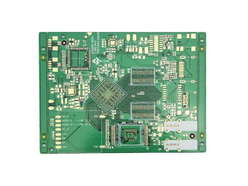
When pressing, PP and copper foil are added on both sides of the double panel, and the high temperature and high pressure are pressed into a multi -layer board. In short, the four -layer board has an inner layer. In terms of process, some circuits will be carved and suppressed in the inner layer. Double -panels can directly cut out the drilling of the factory board. The four -layer board refers to the printing circuit board. PCB is made of four -layer glass fiber, which can reduce the cost of PCB, but the efficiency is very low. Although it is difficult to get the four -layer PCB board by observing the cross section of PCB, few people have such vision. However, you can identify the four -layer board by observing the guide hole. If the same guide hole, or the motherboard or the graphics card can be found on both sides of the PCB, if the position of the guide hole cannot be transmitted, it is a four -layer board. The four -layer circuit board is made of combination on the basis of
Inquiry Now

