 +86 755 2794 4155
  sales@knownpcb.com
-
Shenzhen KNOWNPCB Technology Co., Ltd.
 +86 755 2794 4155
  sales@knownpcb.com
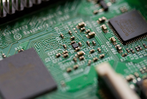
Have you noticed that now more and more of our lighting is using led lighting.What is LED? Compared to the traditional light bulbs, LEDs have lower power consumption, longer lifetime and higher energy efficiency. In the PCB industry,when we say LED PCB, it refers to the pcb used for LED lighting, if you are looking for a suitable LED PCB for your lighting system, this article may bring you something. WHAT ARE LEDS COMPOSED OF?LED is an initial light-emitting diode that produces light when an electric current passes through. LEDs typically have negative and positive electrodes, which generate light in the visible light region.The LEDS are glued to the PCB by soldering process and have electrical connections for lighting.Since light-emitting diodes dissipate a lot of heat when they are in use, when you are designing LED, the metal core is usually the best choice for LED PCB, it is because that it dissipates heat more faster. Among them, the metal material aluminum is the most widely used
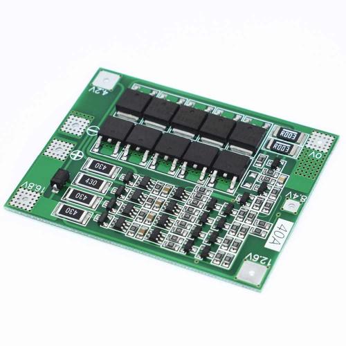
1. Enter the PCB design system and set relevant parameters Set the environmental parameters of the design system based on personal habits, such as the size and type of grid points, the size and type of cursors, etc. Generally, the default values of the system can be used. In addition, parameters such as the size and number of layers of the circuit board need to be set. 2. Generate Import Network Table The network table is a crucial bridge and link between circuit schematic design and printed circuit board design. Network tables can be generated from circuit schematics or extracted from existing electronic circuit board files. When introducing network tables, it is necessary to check and correct errors in the circuit schematic design. 3. Arrange the packaging positions of each component The automatic layout function of the system can be utilized, but it is not very complete and requires manual adjustment of the packaging position of each component. 4. Wiring the circuit board
1. There are many factors to consider when determining the stacking structure of multi-layer PCB boards. In terms of wiring, the more layers there are, the more advantageous it is for wiring, but the cost and difficulty of making boards will also increase accordingly. For manufacturers, the symmetry of the stacked structure is the focus of attention when manufacturing PCB boards, so the selection of the number of layers needs to consider various needs to achieve the best balance. For experienced designers, after completing the pre layout of components, they will focus on analyzing the wiring bottlenecks of PCBs. Analyze the wiring density of the circuit board with other EDA tools; Determine the number and type of signal layers by synthesizing the number and types of signal lines with special wiring requirements, such as differential lines and sensitive signal lines; And then based on Determine the number of internal electrical layers based on the type of power supply, isolation, a
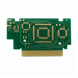
Previously, I worked in a small electronics factory to manually attach PCB board components, which required hundreds of pieces to be attached in a day. The efficiency was very low and could not match that of a mounting machine. Because it is a small factory, there is not enough manpower, and basically every step has been done, so I have some understanding. Firstly, the engineer uses AD software to draw the PCB. After the layout is manually completed, the drawings are handed over to the manufacturer for sampling. Generally, the PCB board and its corresponding steel mesh can be sampled within 7 working days. Then, the device is purchased according to the circuit diagram provided by the engineer. Then, it is the production line. We scrape solder paste on the screen printing table. Align the silk screen of the PCB board with the steel mesh, then fix the steel mesh, and then scrape tin on the steel mesh. Apply the solder paste onto the silk screen on the surface of the PCB board, so tha
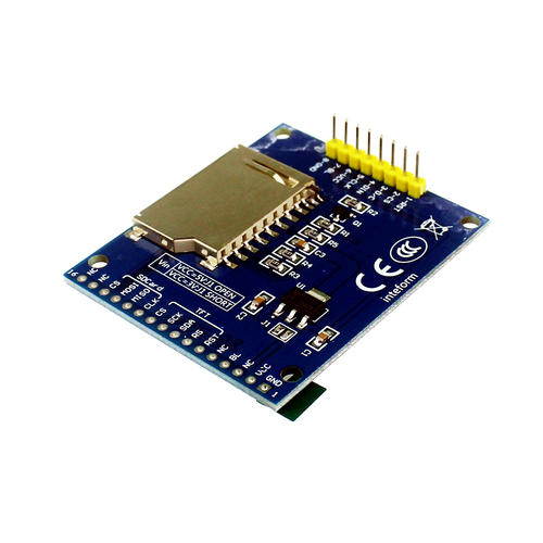
Pcb circuit board manufacturing refers to the trial production of printed circuit boards before mass production, mainly refers to the process that electronic engineers design circuits, complete PCB, and then carry out a small amount of trial production to the factory. This is the Chinese name for PCB, which is printed circuit board, also known as printed circuit board. It is an important electronic component, the support of electronic components, and the electrical connection provider of electronic components. It is called a "printed" circuit board because it is made using electronic printing technology. Pcb circuit board manufacturing refers to the trial production of printed circuit boards before mass production, mainly refers to the process that electronic engineers design circuits, complete PCB, and then carry out a small amount of trial production to the factory. This is the manufacturing of PCB circuit boards. The production quantity of PCB samples usually does not have a spe

1. To prevent short circuits caused by tin penetrating through the component surface through the through hole during PCB wave soldering; Especially when we place the via hole on the BGA pad, we must first make a plug hole and then gild it to facilitate BGA welding. 2. After the surface mounting and component assembly of the electronic factory are completed, the PCB needs to be vacuumed on the testing machine to form negative pressure: 3. Prevent surface solder paste from flowing into the holes, causing false soldering and affecting the installation of PCB circuit boards; 4. Prevent solder beads from popping out during peak soldering, causing short circuits on the PCB circuit board; 5. Avoid flux residue in the through-hole
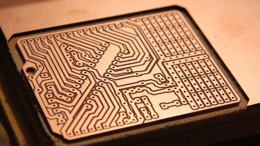
If a PCB circuit board is used in a humid environment, the air contains a large amount of moisture. When the moisture is too high, it will turn into water droplets and fall onto the PCB circuit board. After the water droplets scatter on the circuit board, they will attach to various pins or printed wires of electronic components. After the printed wire is soaked with water droplets, especially when the signal transmission line is relatively small and soaked for a period of time, there will be mold breakage of the printed wire, causing the circuit board to malfunction during the next operation. The causes of circuit board failures caused by moisture are classified into three categories: 1. Causing changes in circuit parameters in the PCB circuit board, leading to PCB circuit board failure; 2. Causing the circuit in the PCB circuit board to be in a short circuit state, causing the PCB circuit board to malfunction; 3. Causing open circuit in signal processing or transmission line
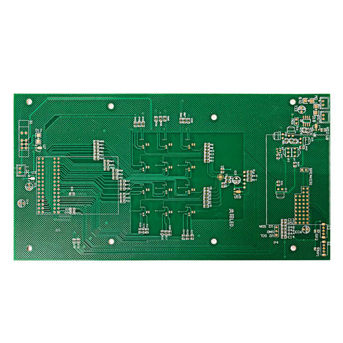
1、 Introduction: With the continuous improvement of human requirements for living environment, the environmental issues involved in PCB production process are particularly prominent. The topic of lead and bromine is currently the most popular; Lead-free and halogen-free technologies will affect the development of PCBs in many ways. Although at present, the changes in the surface treatment process of circuit boards are not significant and may seem distant, it should be noted that long-term slow changes will lead to significant changes. With the increasing demand for environmental protection, the surface treatment process of PCBs is bound to undergo significant changes in the future. 2、 The purpose of surface treatment is to ensure good weldability or electrical performance, which is the most basic purpose of surface treatment. Due to the tendency of copper in nature to exist in the form of oxides in the air, it is unlikely to remain the original copper for a long time, so other tr

The switch regulator used for voltage conversion uses inductance to store energy when it falls. These inductors are usually very large in size and must be positioned in the printed circuit board (PCB) planning of the switch regulator. This task is not difficult, as the current passing through the inductor may change, but it is not an instantaneous change. Changes can only be continuous and usually relatively slow. The switching regulator switches current back and forth between two different paths. This switching is very fast, and the detailed switching speed depends on the duration of the switching edge. The wiring through which switching current flows is called a thermal circuit or AC current path, which conducts current in one switching state and does not conduct current in another switching state. In PCB planning, the thermal circuit area should be small and the path should be short to minimize parasitic inductance in these wiring. Parasitic wiring inductance can generate useles
Inquiry Now

