 +86 755 2794 4155
  sales@knownpcb.com
-
Shenzhen KNOWNPCB Technology Co., Ltd.
 +86 755 2794 4155
  sales@knownpcb.com
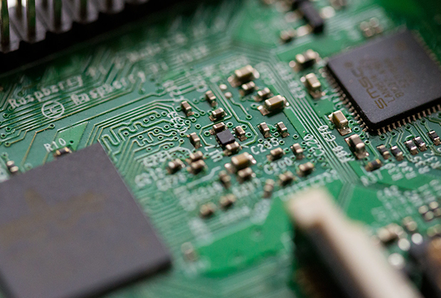
Have you noticed that now more and more of our lighting is using led lighting.What is LED? Compared to the traditional light bulbs, LEDs have lower power consumption, longer lifetime and higher energy efficiency. In the PCB industry,when we say LED PCB, it refers to the pcb used for LED lighting, if you are looking for a suitable LED PCB for your lighting system, this article may bring you something. WHAT ARE LEDS COMPOSED OF?LED is an initial light-emitting diode that produces light when an electric current passes through. LEDs typically have negative and positive electrodes, which generate light in the visible light region.The LEDS are glued to the PCB by soldering process and have electrical connections for lighting.Since light-emitting diodes dissipate a lot of heat when they are in use, when you are designing LED, the metal core is usually the best choice for LED PCB, it is because that it dissipates heat more faster. Among them, the metal material aluminum is the most widely used
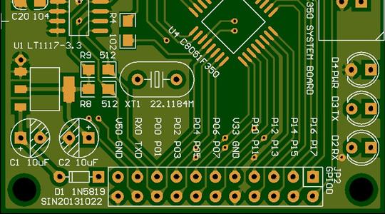
If it is manual welding, it is necessary to develop good habits. Firstly, visually inspect the PCB board before welding, and use a multimeter to check whether key circuits (especially power and ground) are short circuited; Secondly, every time a chip is soldered, use a multimeter to measure whether there is a short circuit between the power supply and ground; In addition, do not throw the soldering iron indiscriminately during soldering. If the soldering tin is thrown onto the solder pins of the chip (especially surface mount components), it is not easy to detect. 2. Open the PCB diagram on the computer, light up the short circuit network, and see where it is closest to where it is most likely to be connected. Pay special attention to internal short circuits in the IC. 3. A short circuit was found. Take a board to cut the thread (especially suitable for single/double layer boards), and after cutting the thread, power on each part of the functional block separately, and exclude som
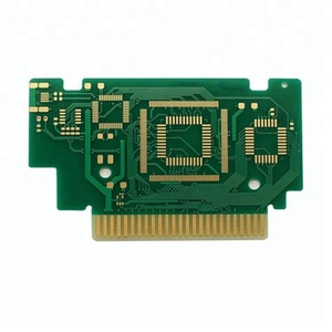
1. Static design Static design refers to the bending or folding that a product only encounters during the assembly process, or the bending or folding that rarely occurs during use. Single sided, double-sided, and multi-layer circuit boards can all successfully achieve folded static design. Usually, for most double-sided and multi substrate designs, the bending radius of the fold should be ten times the thickness of the entire circuit. Circuits with more layers (eight or more) will become very hard and difficult to bend, so there will be no problems. Therefore, for double-sided circuits that require strict bending radius, all copper wires should be set on the same side of the substrate film in the folding area. By removing the film covering on the opposite side, the folded area is approximated as a single sided circuit. 2. Dynamic design The design of dynamic circuits is aimed at the repeated bending that occurs throughout the entire lifecycle of the product, such as the cables o
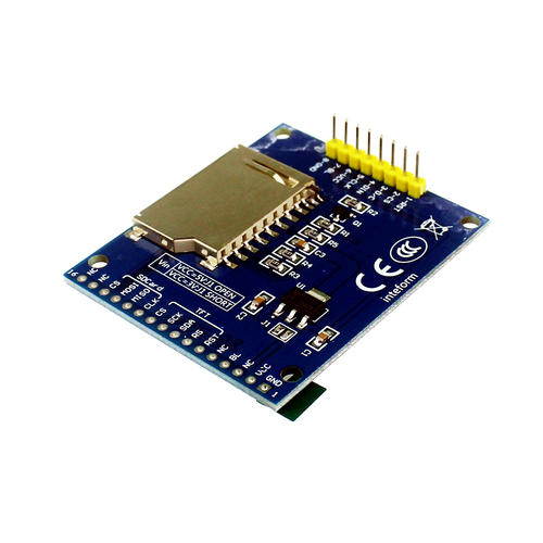
Reduce weight and space Compared to other solutions, flexible printed circuit boards not only provide greater design freedom, but also better space utilization and weight efficiency. Flexible printed circuit boards are thin and lightweight, which can greatly reduce weight and space. For smaller devices, these flexible plates can be folded, creased, and placed in smaller areas to miniaturize the device. This makes flexible circuit boards more suitable for small devices, as they can be installed in areas where rigid circuit boards cannot be installed. flexibility The main advantages of flexible circuit boards are their elasticity and bending ability. Therefore, they can be manipulated in various ways to fit edges, folds, and creases. The flexibility of the circuit board also means that it is more reliable and durable than ordinary PCBs, as it can reduce the impact of vibration and has very few wiring on the circuit board. Minimal wiring eliminates the need for interface connection
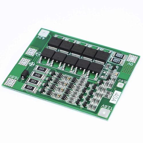
For a PCB sample, please prepare the following information in advance to inquire about it. Being straightforward and not talking nonsense can save you valuable time. More importantly, we are also experts in preparation, and pricing is not at a loss. The PCB circuit board manufacturer has summarized the following points and hopes to help you. Material: What kind of material is required for the design of PCB circuit boards? Currently, FR4 is commonly used, and the commonly used material is epoxy resin peeled fiber cloth board. Board layer: The number of layers for designing PCB circuit boards (the design layers for PCB sampling may vary in price, and the PCB sampling process is similar) Solder resistance color: There are many colors available, which can be selected according to the company's needs, with the commonly used color being green. Screen printing color: The font and border color for screen printing on PCB circuit boards, often selected as white. Copper thickness: Scient
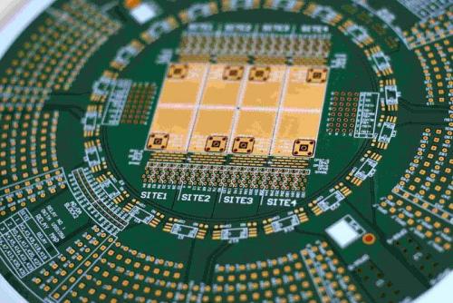
How to check for short circuits on a PCB circuit board? PCB circuit board manufacturers teach you six simple troubleshooting methods. Firstly, computers can easily connect to PCBs, opening up PCB designs, illuminating short-circuit networks, and observing closer areas. Special design should pay attention to internal short circuits in the IC. If it is manual welding, please develop good habits: Before welding, visually inspect the PCB board and use a multimeter to check for short circuits in key circuits (especially power and ground); Welding of finished products for measuring power and ground short circuits using a multimeter to various chips; Do not throw soldering iron randomly during welding. If solder is thrown onto the solder feet of the chip (especially for surface mounted components), it will be difficult to find it. Analyze the main instruments using a short circuit positioning system If there is a BGA processing chip, as all tin points are covered by the processing

Can be high-density For many years, the high-density of printed boards has been able to develop correspondingly with the improvement of integrated circuit integration and the advancement of installation technology. high reliability Through a series of inspection, testing, and aging tests, it is possible to ensure that PCBs can work reliably for a long time (usually with a lifespan of 20 years). Designability The requirements for various properties of PCBs (electrical, physical, chemical, mechanical, etc.) can be achieved through design standardization and standardization. This design has a short time and high efficiency. Producibility PCB adopts modern management, which can achieve standardization, scale (quantity), and automated production, thereby ensuring the consistency of product quality. [2] Testability We have established relatively complete testing methods and standards, which can be used to detect and evaluate the qualification and service life of PCB products thr
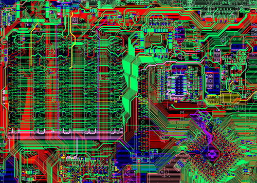
1. Spacing between wires For the processing capacity of Shenzhen PCB manufacturers, the minimum distance between wires should not be less than 3mil. The minimum line distance is also the distance from line to line and from line to pad. From a production perspective, if conditions permit, the larger the better, with a common one being 10mil. 2. Pad aperture and pad width In terms of the processing capacity of PCB manufacturers in Shenzhen, if the pad aperture is mechanically drilled, the minimum should not be less than 0.15mm, and if laser drilling is used, the minimum should not be less than 4mil. The aperture tolerance varies slightly depending on the plate, and can generally be controlled within 0.05mm. The minimum width of the welding pad should not be less than 0.2mm. If copper is laid on a large area, there usually needs to be an internal shrinkage distance of 20mil from the edge of the board. In the PCB design and manufacturing industry, in general, due to mechanical cons
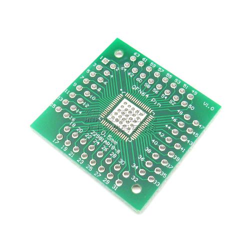
Firstly, a PCB or GERBER file needs to be provided, which should include plate making instructions - including specific requirements such as board layers, materials, solder pad process, ink color, etc. Below, we will provide a detailed explanation of some of the main parameters. Material: It is necessary to explain what kind of material is required for PCB production. Currently, the most common method is to use FR4, which is mainly made of epoxy resin peeled fiber cloth board. Board layer: It is necessary to specify the number of layers for making PCB boards. (The production layers of PCB boards vary, and the price will also vary. The sampling process for PCB circuit boards is very similar.) Solder resistance color: There are many colors available, which can also be selected according to requirements, usually green. Screen printing color: The font and border color for screen printing on a PCB are generally selected as white. Copper thickness: Generally, the scientific calculat
Inquiry Now

