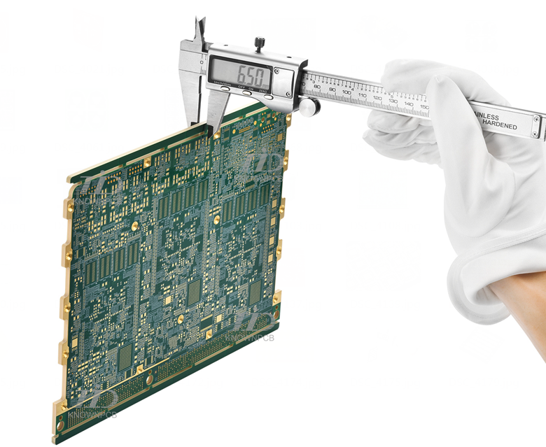
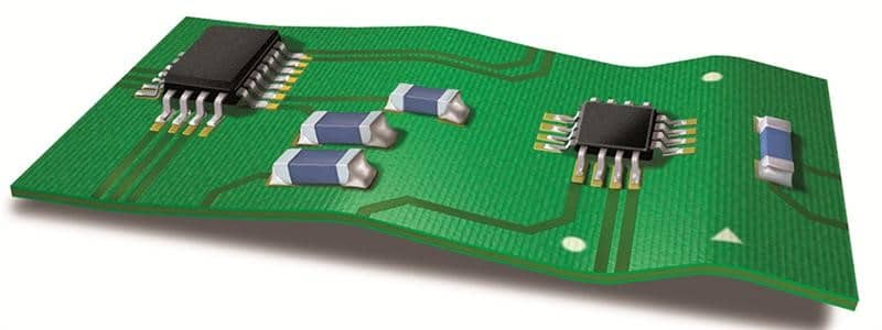
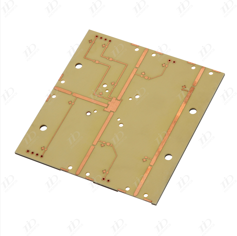
Ultra thin PCBs have unique specifications that make them highly suitable for specific applications where space and flexibility are of utmost importance. The thickness of an ultra thin PCB is one of its most defining characteristics. Typically, these PCBs can have a thickness ranging from as little as 0.1mm to a few tenths of a millimeter. This extremely thin profile allows them to be used in applications where space is severely limited. For example, in modern smartphones and tablets, ultra thin PCBs enable the device manufacturers to make the products thinner and more compact. They can be easily integrated into the slim body of the device without adding significant bulk. The materials used in ultra thin PCBs are carefully selected. Special substrate materials are often employed that have both good electrical properties and the required mechanical strength at such thin dimensions. For instance, flexible materials like polyimide are commonly used. Polyimide based substrates offer
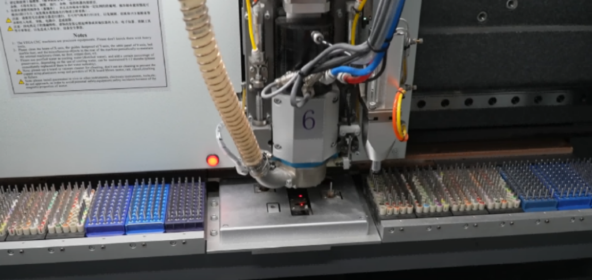
There are various ways to split PCB boards, and the following will introduce several common ways of splitting: 1. Milling and cutting of PCB boards: Using a CNC milling machine, cut grooves on the PCB board and use a rotating tool or milling cutter to cut the board into small pieces, suitable for various shapes and sizes of boards. 2. Punching and Splitting: Through die-cutting technology, holes are pressed on the PCB board, and then force is applied to break the board, achieving the splitting operation, suitable for rectangular and regular shaped boards. 3. V-knife board splitting: Use a special V-shaped blade to cut V-shaped slots on the PCB board, then apply force to break the board and separate it into small pieces, suitable for thinner boards and situations with high precision requirements. 4. Laser board splitting: Using laser cutting technology, precise cutting can be performed on PCB boards to achieve complex shapes and high-precision board splitting requirements, suita
Printed Circuit Boards (PCBs) are essential components in electronic devices, and anti - oxidation treatment of PCBs is of great significance to ensure their long - term performance and reliability. The main purpose of PCB anti - oxidation treatment is to prevent the copper surfaces on the PCB from oxidizing. Copper is widely used in PCBs for its excellent electrical conductivity. However, copper is highly susceptible to oxidation when exposed to air, moisture, and other environmental factors. Oxidation of copper can form copper oxide or other copper compounds, which can increase the resistance of the circuit, degrade the electrical performance of the PCB, and even lead to potential failure of the entire electronic system. There are several common methods for PCB anti - oxidation treatment. One of the most widely used techniques is the application of anti - oxidation coatings. These coatings can be organic or inorganic materials. Organic coatings usually contain polymers with cer
Specific size PCB A specific size PCB (Printed Circuit Board) plays a crucial role in various electronic devices, and its design and manufacturing are carefully tailored to meet specific requirements. When dealing with a specific size PCB, the first consideration is the physical dimensions. These dimensions are determined by the available space within the device it will be installed in. For example, in a handheld consumer electronics device like a smartwatch, the PCB size is extremely limited. It needs to fit within the tiny casing while accommodating all the necessary components such as the microprocessor, memory chips, sensors, and connectivity modules. In contrast, in a larger device like a desktop computer motherboard, the PCB size can be much larger to provide enough space for numerous components, expansion slots, and connectors. The size also affects the routing of the traces on the PCB. In a small size PCB, the traces need to be carefully designed to avoid short circuits an
The Influence of Surface Treatment Materials on PCBs Surface treatment materials have a profound impact on the performance, reliability, and lifespan of PCBs. Different surface treatment methods are employed to meet various requirements in the electronics industry. One of the most common surface treatment materials is HASL (Hot Air Solder Leveling). HASL involves coating the PCB surface with a thin layer of solder alloy using hot air. This treatment provides excellent solderability as the solder layer allows for easy formation of reliable solder joints. It also offers good protection against oxidation during the storage and assembly process of the PCB. However, HASL has some limitations. The thickness of the solder layer may vary, which can affect the precision of fine pitch components. Additionally, the process may leave some residues that need to be carefully cleaned to avoid potential short circuits. Another widely used surface treatment is OSP (Organic Solderability Preservati
High - thermal - conductivity printed circuit boards (PCBs) play a crucial role in electronic devices where efficient heat dissipation is essential. These PCBs are designed to manage heat effectively, thereby improving the reliability and performance of the overall system. The materials used in high - thermal - conductivity PCBs are the key to their heat - dissipating capabilities. One common approach is to use metal - based substrates. For example, aluminum - based PCBs are widely used. The aluminum core provides an excellent heat - conducting path. The copper layers on the PCB are laminated onto the aluminum substrate, allowing heat generated by the components to be quickly transferred to the aluminum and then dissipated into the surrounding environment. Another option is to use ceramic - based materials. Ceramic substrates have high thermal conductivity and can withstand high temperatures. They are often used in high - power applications such as power amplifiers and LED lightin
1. Introduction to PCB Industry Standards The printed circuit board (PCB) industry is highly regulated by a set of standards that ensure the quality, reliability, and compatibility of PCBs in various applications. These standards are developed by international organizations, industry associations, and regulatory bodies. 2. Design and Layout Standards Component Placement and Spacing One of the key aspects of PCB design standards is component placement and spacing. There are specific rules regarding how close components can be placed to each other. For example, to prevent short - circuits and ensure proper heat dissipation, there are minimum distances specified between different types of components. Surface - mount components may have different spacing requirements compared to through - hole components. In addition, the orientation of components is also standardized in some cases. This is to ensure consistent manufacturing processes and ease of inspection. For example, polarized
PCB board materials are classified based on several factors, including their performance characteristics, intended applications, and manufacturing requirements. 1. Based on Substrate Materials One of the main ways to classify PCB materials is by the type of substrate used. The most common substrate material is fiberglass reinforced epoxy resin, known as FR 4. FR 4 boards have good mechanical strength, electrical insulation properties, and are suitable for a wide range of applications. They can withstand relatively high temperatures during the soldering process and have stable dielectric properties. Another type of substrate is polyimide, which is used in high temperature and high frequency applications. Polyimide based PCBs can operate at much higher temperatures than FR 4 boards and have excellent dielectric properties at high frequencies. They are often used in aerospace, military, and some high end electronics applications where temperature and frequency stability are crucial.
A high-capacity energy storage power source is essential in various applications where a large amount of energy needs to be stored and supplied reliably. One of the key areas where it is highly valuable is in off-grid power systems. For example, in remote areas where access to the main power grid is limited or unavailable, such as mountain cabins or rural villages, a high-capacity energy storage power source can store energy from renewable sources like solar panels or wind turbines. This stored energy can then be used to power electrical appliances, lighting, and other essential equipment throughout the day and night. In the event of bad weather or low renewable energy generation, the large energy storage capacity ensures that there is still a sufficient supply of power to meet the basic needs. Another application is in emergency backup power systems. During power outages caused by natural disasters, grid failures, or other unforeseen circumstances, a high-capacity energy storage
PCB (Printed Circuit Board) board welding is a critical process in electronics manufacturing, and there are several national standards in place to ensure the quality and reliability of the soldered connections. 1. Soldering Material Standards The choice of soldering materials, such as solder paste and solder wire, is governed by specific standards. For solder paste, its composition, including the ratio of tin, lead (in lead containing solders), and other alloying elements, is precisely defined. The viscosity of the solder paste is also a crucial parameter as it affects the printing accuracy and the ability to hold components in place during reflow soldering. In the case of solder wire, its diameter and the content of flux are standardized. Flux helps in cleaning the metal surfaces to be soldered and promotes the wetting of the solder, ensuring a good bond. The flux content and its activity level are specified to meet different soldering requirements, such as for through hole comp
A power electronic PCB (Printed Circuit Board) is a crucial component in various electrical and electronic systems that deal with the control and conversion of electrical power. It is designed to handle high voltages and currents, making it essential for applications such as power supplies, motor drives, and renewable energy systems. The design of a power electronic PCB requires careful consideration of several factors. One of the key aspects is the layout. The components on the PCB need to be arranged in a way that minimizes the length of the power traces to reduce resistance and inductance. This is crucial as it helps in minimizing power losses and improving the efficiency of the power conversion process. For example, in a power supply PCB, the placement of the capacitors, inductors, and power transistors is carefully planned to ensure smooth flow of current and voltage. Another important consideration is the thermal management. Power electronic components generate a significan
High-precision printed circuit boards (PCBs) are essential for applications that demand exceptional electrical performance and reliability. These PCBs require strict specification requirements to ensure accurate and consistent functionality. One of the key requirements for high-precision PCBs is tight dimensional tolerance. The board dimensions, hole locations, and trace widths and spacings must be controlled within very narrow limits to ensure proper component placement and signal integrity. This often requires advanced manufacturing processes and precision machinery. High-precision PCBs also require excellent surface finish. The copper surfaces must be smooth and free from defects to ensure good solderability and electrical conductivity. Common surface finishes for high-precision PCBs include immersion gold, electroless nickel/immersion gold (ENIG), and organic solderability preservative (OSP). Signal integrity is another critical aspect of high-precision PCBs. The traces must
Printed Circuit Boards (PCBs) with standard specifications play a crucial role in various electronic applications. These PCBs are designed to meet common industry requirements and offer reliable performance. The standard specification PCB typically consists of a rigid or flexible substrate material, such as FR-4 glass epoxy or polyimide. The substrate provides mechanical support and electrical insulation for the components and traces on the board. The copper traces on a standard PCB are laid out according to the circuit design, connecting the various components such as resistors, capacitors, integrated circuits, and connectors. The trace width and spacing are usually determined based on the current-carrying capacity and signal integrity requirements. Standard PCBs often have a defined number of layers, ranging from single-sided to multilayer configurations. Single-sided PCBs have components and traces on one side only, while double-sided PCBs have components and traces on both s
The PCB fixture test is a common method used to test the functionality and quality of printed circuit boards (PCBs). This test involves using a custom-made fixture that holds the PCB in place and provides electrical connections for testing. The fixture is designed to fit the specific dimensions and layout of the PCB being tested. It typically consists of a base plate, a set of alignment pins, and a series of spring-loaded probes or contacts. The alignment pins ensure that the PCB is properly positioned in the fixture, while the probes or contacts make electrical connections to the PCB's test points. Once the PCB is inserted into the fixture, the test equipment is connected to the fixture's electrical contacts. The test equipment then applies various electrical signals and measurements to the PCB to determine if it is functioning properly. This may include testing for continuity, resistance, capacitance, and other electrical parameters. One of the main advantages of the PCB fixtu
The PCB flying probe test is a method used to test the electrical functionality of printed circuit boards (PCBs). This test is performed using specialized equipment that consists of multiple probes that can move independently and make contact with the PCB at different points. The flying probe test works by sending electrical signals through the PCB and measuring the responses at various points. The probes are programmed to move to specific locations on the PCB and make contact with the conductive traces or pads. The test equipment then applies electrical stimuli, such as voltage or current, and measures the resulting responses, such as resistance, capacitance, or inductance. One of the main advantages of the flying probe test is its flexibility. Since the probes can move independently, they can test PCBs of different sizes and shapes without the need for custom fixtures or test jigs. This makes the flying probe test ideal for small-volume production runs or for testing prototypes
PCB electroplating gold is a process that deposits a layer of gold onto the surface of a printed circuit board (PCB) through an electrochemical reaction. This process is commonly used to improve the electrical conductivity, solderability, and corrosion resistance of PCBs. The electroplating gold process typically involves several steps. First, the PCB is cleaned and prepared to ensure a clean and smooth surface for the gold plating. Then, a thin layer of a conductive material, such as copper or nickel, is applied to the PCB to provide a base for the gold plating. Next, the PCB is immersed in an electroplating bath containing a gold salt solution and an electrical current is passed through the bath. The electrical current causes the gold ions in the solution to be reduced and deposited onto the surface of the PCB, forming a layer of gold. One of the main advantages of electroplating gold is that it can provide a very thin and uniform layer of gold on the PCB surface. This can be b
PCB gold immersion, also known as electroless gold plating, is a surface finishing process used in printed circuit board (PCB) manufacturing. This process involves depositing a thin layer of gold onto the surface of the PCB to enhance its electrical conductivity, solderability, and corrosion resistance. The gold immersion process typically begins with a cleaning step to remove any contaminants from the PCB surface. This is followed by an activation step, where a catalyst is applied to the surface to promote the adhesion of the gold layer. Next, the PCB is immersed in a gold plating solution, which contains a reducing agent and a gold salt. The reducing agent causes the gold ions in the solution to be reduced and deposited onto the PCB surface, forming a thin layer of gold. One of the main advantages of gold immersion is its ability to provide a uniform and smooth gold layer on the PCB surface. This is important for ensuring good electrical contact and solderability. Gold immersio
PCB Gold Plating Gold plating on printed circuit boards (PCBs) is a common surface finish that offers several advantages. This process involves depositing a thin layer of gold onto the copper traces and pads of the PCB. One of the main benefits of gold plating is its excellent electrical conductivity. Gold is a highly conductive metal, which helps to reduce signal loss and improve the performance of high-frequency and high-speed circuits. It also has a low contact resistance, ensuring reliable electrical connections. Another advantage of gold plating is its corrosion resistance. Gold is highly resistant to oxidation and corrosion, protecting the copper traces on the PCB from environmental factors such as moisture, chemicals, and temperature changes. This makes gold plating suitable for use in harsh environments or applications where long-term reliability is required. Gold plating also offers good solderability. The gold layer provides a clean and stable surface for soldering, ens
PCB Immersion Gold (ENIG) PCB immersion gold, also known as electroless nickel immersion gold (ENIG), is a popular surface finish for printed circuit boards (PCBs). This process offers several advantages that make it a preferred choice in many applications. One of the main benefits of ENIG is its excellent solderability. The gold layer provides a clean and stable surface for soldering, ensuring reliable electrical connections. It also has a low contact resistance, which is crucial for high-frequency and high-speed applications. Another advantage of ENIG is its corrosion resistance. The nickel layer acts as a barrier against oxidation and corrosion, protecting the copper traces on the PCB. This makes ENIG suitable for use in harsh environments or applications where long-term reliability is required. ENIG also offers good flatness and planarity, which is important for fine-pitch components and high-density packaging. The smooth surface of the gold layer allows for easy placement an
Storage Device PCB The Printed Circuit Board (PCB) of a storage device plays a vital role in the functionality and performance of the device. Whether it's a hard disk drive, solid-state drive, or other storage medium, the PCB is responsible for controlling and managing the data storage and retrieval processes. The design of a storage device PCB is tailored to meet the specific requirements of the storage technology. For example, in a hard disk drive PCB, there are components such as the motor controller, read/write head amplifier, and interface controller. These components work together to manage the movement of the disk platters and the transfer of data between the drive and the host system. In a solid-state drive PCB, on the other hand, there are flash memory controllers, power management circuits, and interface connectors. The flash memory controllers are responsible for managing the read and write operations to the NAND flash memory chips, while the power management circui
Inquiry Now