 +86 755 2794 4155
  sales@knownpcb.com
-
Shenzhen KNOWNPCB Technology Co., Ltd.
 +86 755 2794 4155
  sales@knownpcb.com
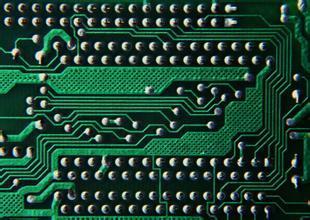
PCB (Printed Circuit Board) and PCBA (Printed Circuit Board Assembly) are related but not the same category of items in the electronics manufacturing field. A PCB is a physical board that serves as a foundation for electronic components. It is made of a non - conductive substrate, usually fiberglass, with conductive copper traces printed or etched on it. These copper traces act as electrical pathways, allowing signals and power to flow between different parts of the circuit. PCBs come in various types, such as single - sided, double - sided, and multi - layer PCBs. Single - sided PCBs have copper traces on only one side of the board, while double - sided PCBs have traces on both sides, connected by vias. Multi - layer PCBs consist of multiple layers of copper traces separated by insulating layers, which can accommodate more complex circuits. On the other hand, PCBA refers to a fully assembled PCB. Once a PCB is fabricated, electronic components such as resistors, capacitors, inte

PCB layout is a critical step in the design of printed circuit boards. It involves arranging the electronic components on the board and routing the electrical connections between them. A well-designed PCB layout can improve the performance, reliability, and manufacturability of an electronic device. The first step in PCB layout is to determine the placement of the major components. This includes the microcontroller, power supply, connectors, and other key components. The placement should be based on factors such as signal flow, power distribution, and thermal management. Once the major components are placed, the smaller components can be added. These may include resistors, capacitors, diodes, and other discrete components. The placement of these components should be optimized to minimize the length of the traces and to reduce the risk of interference. Routing the traces is the next step in PCB layout. The traces should be routed in a way that minimizes crosstalk and electromagne
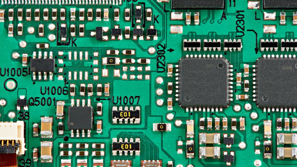
Power PCBs are specifically designed to handle the distribution and management of power in electronic systems. These PCBs play a critical role in ensuring the reliable and efficient operation of various devices, from power supplies and motor drives to high-power industrial equipment.The design of power PCBs focuses on several key aspects. Firstly, they need to have a low impedance to minimize power losses during transmission. This is achieved through the use of thick copper traces and appropriate layer stacking. The layout is carefully planned to reduce the length of power paths and avoid sharp bends or corners that could increase resistance.Thermal management is also crucial for power PCBs. High-power components such as power transistors and diodes generate a significant amount of heat, and the PCB must be designed to dissipate this heat effectively. This may involve the use of heat sinks, thermal vias, and special laminate materials with good thermal conductivity. power PCBs need to
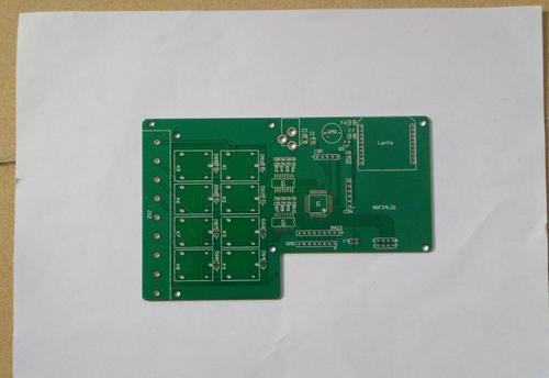
Small-size PCBs, also known as printed circuit boards, are widely used in various electronic devices where space is limited. These compact PCBs are designed to fit into small form-factor products such as wearable devices, miniature sensors, and some handheld electronics. The reduced size requires precise manufacturing techniques and careful component placement. Manufacturers of small-size PCBs often use advanced technologies like high-density interconnect (HDI) to increase the number of connections and components that can be integrated within a limited area. This allows for the creation of more complex circuitry without sacrificing space. For example, in a smartwatch PCB, components like the microprocessor, memory chips, and sensors need to be arranged in a highly efficient manner to fit within the tiny enclosure. The materials used for small-size PCBs also play a crucial role. They need to be lightweight and have good electrical properties. Flame-retardant materials are often pr
New energy printed circuit boards are integral to the development and operation of various renewable energy systems and emerging energy storage technologies. In the field of solar power generation, PCBs are used in solar inverters. Solar inverters convert the direct current (DC) electricity generated by solar panels into alternating current (AC) electricity that can be fed into the power grid or used to power local electrical loads. The PCBs in solar inverters are responsible for controlling the power conversion process, ensuring high efficiency and stable output. They need to handle high voltages and currents while maintaining accurate monitoring of the electrical parameters such as voltage, current, and power factor. For example, advanced PCBs incorporate intelligent power management chips that can optimize the conversion efficiency based on real-time solar irradiation and load conditions. When it comes to energy storage systems like lithium-ion batteries used in electric vehic
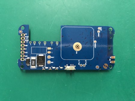
IoT printed circuit boards are the backbone of the vast and complex Internet of Things ecosystem. They are designed to enable seamless connectivity and data exchange among numerous devices spread across different environments. In an IoT system, PCBs need to be highly adaptable to handle a diverse range of sensors and communication modules. For example, in a smart city application, IoT PCBs in streetlights may incorporate light sensors to adjust brightness according to ambient light conditions, as well as cellular or LoRaWAN communication modules to send data about energy consumption and maintenance needs back to a central control system. Similarly, in industrial IoT settings, PCBs in factory equipment can connect temperature sensors, vibration sensors, and other monitoring devices to the cloud for predictive maintenance and process optimization. Power efficiency is a critical factor for IoT PCBs. Since many IoT devices are battery-powered or rely on energy harvesting techniques,
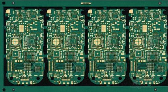
Printed circuit boards for smart home systems are becoming increasingly important as smart home technology continues to evolve and penetrate our daily lives. Smart home PCBs are designed to integrate and control a wide variety of functions within a home environment. One of the main characteristics of smart home PCBs is their ability to support multiple communication protocols. They need to be able to communicate with different devices such as smart thermostats, smart lighting systems, security cameras, and smart locks. For instance, they may use Wi-Fi, Bluetooth, Zigbee, or Z-Wave protocols to establish connections and enable seamless interaction between these devices. This allows homeowners to control all their smart home appliances and systems from a single interface, like a smartphone app or a central control panel. The miniaturization of components on smart home PCBs is also a significant trend. As smart home devices are often designed to be sleek and unobtrusive in a home's
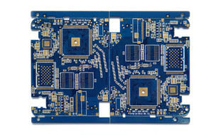
Military printed circuit boards (PCBs) play a vital and unique role in defense applications. These PCBs are designed to meet extremely high standards due to the critical nature of military equipment and operations. Firstly, in terms of reliability, military PCBs must be able to function flawlessly under harsh and diverse conditions. They may be exposed to extreme temperatures, ranging from the intense heat of deserts to the freezing cold of high-altitude or polar regions. They also need to withstand significant mechanical vibrations and shocks that occur during transportation, deployment, or in combat scenarios. For example, in military vehicles, aircraft, or naval vessels, the PCBs installed in communication systems, navigation devices, and weapon control systems must remain operational without any failures. The materials used for military PCBs are carefully selected for their durability and performance. High-quality substrates with excellent thermal management properties are em
Printed Circuit Board (PCB) rework and repair is an important process in the electronics manufacturing industry. It involves the correction of defects or the modification of existing PCBs to meet new requirements. One of the main reasons for PCB rework is the occurrence of defects during the manufacturing process. These defects can range from simple soldering issues to more complex problems such as component failures or incorrect placement. Reworking the PCB allows for the correction of these defects without having to scrap the entire board, saving time and money. Another reason for PCB rework is the need to make modifications to existing PCBs. This can be due to design changes, component upgrades, or customer requests. Reworking the PCB allows for these modifications to be made quickly and efficiently, without having to manufacture a new board from scratch. The process of PCB rework typically involves several steps. First, the defective or modified area of the PCB is identified
Printed Circuit Board (PCB) testing is a crucial step in the manufacturing process to ensure the quality and functionality of the boards. There are several types of PCB testing methods, each with its own advantages and applications. One common method of PCB testing is visual inspection. This involves examining the board for any obvious defects such as missing components, incorrect placement, or solder bridges. Visual inspection can be done manually or with the help of automated optical inspection (AOI) systems. AOI systems use cameras and image processing software to detect defects with high accuracy and speed. Another important testing method is electrical testing. This involves applying electrical signals to the PCB and measuring the responses to ensure that the circuits are functioning properly. Electrical testing can include continuity testing, which checks for proper connections between components, and functional testing, which verifies the operation of the entire circuit.
Printed Circuit Board (PCB) Surface Mount Technology (SMT) processing is a crucial step in the manufacturing of electronic devices. SMT involves the placement of surface mount components onto the PCB using specialized equipment and processes. The first step in SMT processing is the preparation of the PCB. This includes cleaning the board to remove any contaminants and applying a solder paste to the areas where the components will be placed. The solder paste is a mixture of fine solder particles and flux, which helps to ensure good solder connections. Next, the surface mount components are placed onto the PCB using a pick-and-place machine. These machines are highly automated and can place thousands of components per hour with great precision. The components are held in place on the PCB by the tackiness of the solder paste. Once the components are placed, the PCB is passed through a reflow oven. The reflow oven heats the solder paste to a specific temperature, causing it to melt
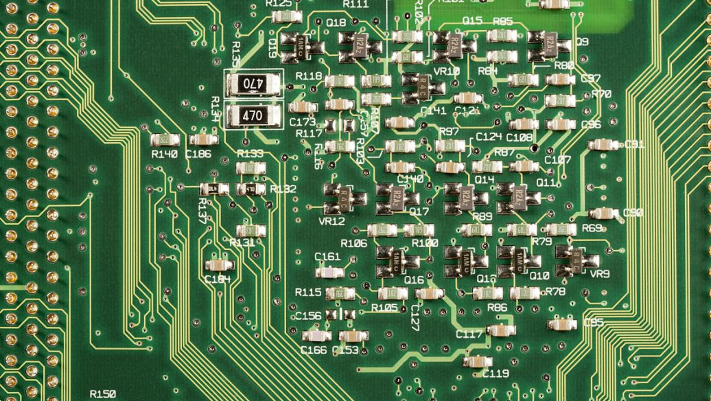
Printed Circuit Board (PCB) mass production is a complex and highly specialized process that requires precision, efficiency, and quality control. The goal of PCB mass production is to produce large quantities of PCBs in a cost-effective and timely manner while maintaining high quality standards. The first step in PCB mass production is the design and layout of the circuit board. This involves creating a detailed schematic diagram and then converting it into a physical layout using specialized software. The layout must take into account factors such as component placement, signal routing, and power distribution to ensure optimal performance and reliability. Once the design is complete, the next step is to manufacture the PCBs. This typically involves a series of processes such as etching, drilling, plating, and printing. Etching is used to remove unwanted copper from the board, while drilling creates holes for components and vias. Plating is then used to add conductive layers to t
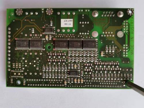
Low-cost PCB materials are of great interest in the electronics industry, especially for mass-produced consumer electronics and applications where cost is a major constraint. One of the commonly used low-cost PCB materials is phenolic paper laminate. It is made from paper impregnated with phenolic resin. This material has relatively low manufacturing costs due to the inexpensive raw materials and simple manufacturing process. It is suitable for applications where the electrical and mechanical requirements are not extremely high, such as simple electronic toys, basic consumer electronics with low power consumption, and some educational electronics kits. Another low-cost option is FR-4, which is a fiberglass-reinforced epoxy laminate. It has been widely used in the electronics industry for decades. FR-4 offers a good balance between cost and performance. It has acceptable electrical and mechanical properties for many mid-range applications. It can be used for circuit boards in compu
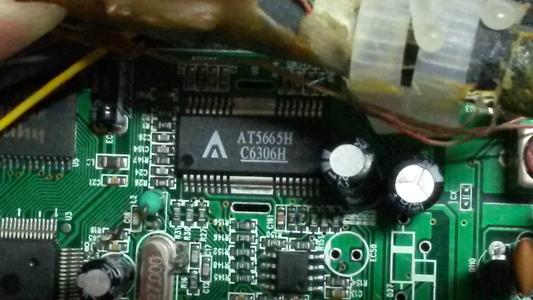
The choice of environmentally friendly PCB materials is becoming increasingly crucial in the electronics industry. Traditional PCB materials often contain harmful substances that can have a negative impact on the environment and human health during manufacturing, use, and disposal. One of the main environmentally friendly alternatives is the use of lead-free solders. Lead is a toxic heavy metal, and replacing it with lead-free alloys helps to reduce the environmental pollution associated with PCB production and recycling. Another important aspect is the selection of substrates. Biodegradable or recyclable substrates are being explored. For example, some plant-based materials or polymers that can be broken down more easily than traditional fiberglass substrates are being considered. These materials not only reduce the burden on landfills but also have a lower carbon footprint during production. Additionally, the use of halogen-free materials is gaining popularity. Halogens, such as
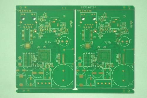
PCB assembly is a comprehensive process that transforms a bare printed circuit board into a functional electronic device. It encompasses multiple steps and techniques to ensure the correct integration of components and the proper operation of the circuitry. The first stage is usually the component placement. This can be done either manually by trained technicians for small production runs or by highly automated surface mount technology (SMT) machines for mass production. SMT allows for the rapid and precise placement of small surface mount components directly onto the surface of the PCB. After component placement, soldering is a critical step. Reflow soldering is commonly used for SMT components, where the PCB is passed through a heated chamber to melt the solder paste and form reliable connections. For through-hole components, as mentioned earlier, wave soldering or selective soldering may be applied. The PCB assembly process also includes quality assurance measures. Automated o
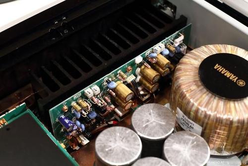
PCB through-hole component insertion processing is a crucial step in the manufacturing of printed circuit boards. It involves the precise placement of various electronic components into the holes drilled on the PCB. The process begins with the preparation of the components. These components, such as resistors, capacitors, and integrated circuits with leads, need to be sorted and inspected to ensure their quality and correct specifications. Then, the PCB is properly aligned and held in place. Skilled technicians or automated machines carefully insert the leads of the components into the corresponding holes on the PCB. The leads are usually bent or clinched on the other side of the board to secure the components in position. Accuracy is of utmost importance in this process. Incorrect insertion can lead to electrical shorts, open circuits, or unreliable connections. To achieve high accuracy, specialized tools and fixtures are often used. For example, insertion machines can be progra
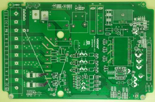
In the world of electronics, printed circuit boards (PCBs) play a crucial role in connecting and supporting electronic components. As technology advances, there is an increasing demand for larger-sized PCBs to accommodate more complex circuits and components. A large-sized PCB offers several advantages. Firstly, it provides more space for placing a greater number of components. This is particularly useful in applications where a large amount of circuitry is required, such as in industrial control systems, telecommunications equipment, and medical devices. With more space available, designers can optimize the layout of the components to improve performance and reliability. Secondly, a large PCB can handle higher power and current levels. The increased surface area allows for better heat dissipation, reducing the risk of overheating and component failure. This is essential in power electronics applications where high currents and voltages are involved. Moreover, large-sized PCBs c

Printed circuit boards (PCBs) come in a variety of shapes and sizes to meet the diverse needs of different applications. The specifications of these PCBs play a crucial role in determining their performance and suitability for a particular use. One common shape for PCBs is the rectangular shape. Rectangular PCBs are widely used in many electronic devices due to their simplicity and ease of manufacturing. They can be designed with different dimensions and thicknesses to accommodate different components and circuit requirements. The specifications of rectangular PCBs typically include the length, width, thickness, number of layers, and material used. Another popular shape is the circular PCB. Circular PCBs are often used in applications where space is limited or where a unique aesthetic is desired. They can be designed with different diameters and can be single-sided, double-sided, or multilayered. The specifications of circular PCBs may include the diameter, thickness, number of l
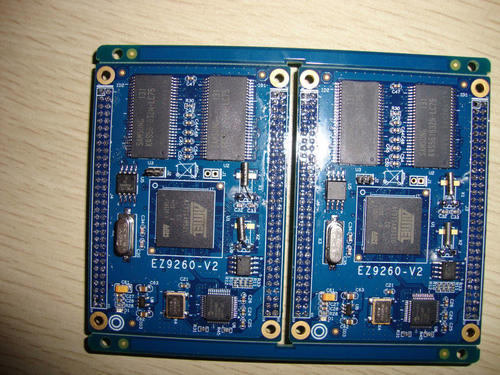
PCB surface treatment is a critical step in the manufacturing of printed circuit boards. It involves applying a thin layer of material to the surface of the copper traces and pads on the PCB. There are several common types of PCB surface treatment, each with its own characteristics and purposes. One of the most widely used surface treatments is hot air solder leveling (HASL). In this process, the PCB is dipped into a molten solder bath and then passed through a hot air blower. This creates a thin, smooth layer of solder on the copper surfaces. HASL provides good solderability and is relatively inexpensive. However, it may have some limitations in terms of flatness and thickness control, especially for fine-pitch components. Another popular surface treatment is electroless nickel immersion gold (ENIG). It involves depositing a layer of nickel on the copper surface followed by a thin layer of gold. ENIG offers excellent corrosion resistance and good electrical conductivity. It is s
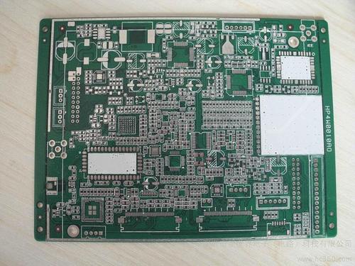
PCB legend, also known as PCB component overlay or PCB silkscreen legend, is an important aspect of printed circuit board design. It consists of text and graphical symbols that are printed on the surface of the PCB. The main role of the PCB legend is to provide information about the components and their locations on the PCB. It helps in the assembly process by allowing technicians to quickly identify where each component should be placed. For example, the legend will show the position of resistors, capacitors, integrated circuits, and other components with their corresponding designators. The PCB legend can also include additional information such as the polarity of components. For polarized components like diodes and electrolytic capacitors, the legend will indicate the correct orientation. This is crucial as incorrect placement of polarized components can lead to malfunction or even damage to the PCB. the legend can provide information about test points, jumper settings, and oth
Inquiry Now

