 +86 755 2794 4155
  sales@knownpcb.com
-
Shenzhen KNOWNPCB Technology Co., Ltd.
 +86 755 2794 4155
  sales@knownpcb.com
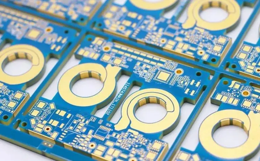
Heavy copper PCBs have high current-carrying and thermal conductivity, with wide industrial use, but face manufacturing/cost/design challenges needing specific guidelines.
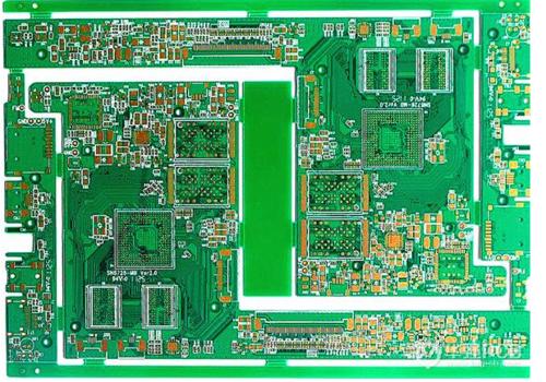
The Sino - US trade situation has been a topic of global concern, and its implications span across numerous industries. The Printed Circuit Board (PCB) industry, a fundamental part of the electronics value chain, is no exception. The relationship between Sino - US trade and the PCB industry is complex, with various factors at play that can influence the industry's growth, market dynamics, and competitive landscape. Direct Impact on Trade Volumes One of the most immediate aspects to consider is the direct effect on trade volumes. China is a dominant force in the global PCB market, accounting for over 50% of the world's production capacity. The United States, on the other hand, is a major consumer of electronics products that rely on PCBs. When trade tensions rise, such as the imposition of tariffs, it directly impacts the cost of PCB products traded between the two countries. For instance, during the previous rounds of Sino - US trade disputes, the US imposed tariffs on a range o
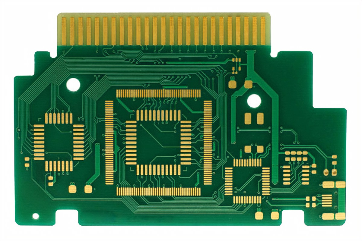
The gold finger possess excellent electrical conductivity, ensuring efficient signal and current transmission. Additionally, it offer strong corrosion resistance, effectively withstanding oxidation and corrosion. Lastly, they exhibit robust mechanical strength, capable of enduring insertion, removal, and pressure.
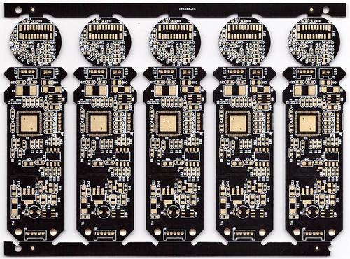
In the era of 5G technology, 5G PCB (Printed Circuit Board) boards play a pivotal role in ensuring the seamless operation of high - speed communication devices. These boards are the unsung heroes behind the functionality of 5G smartphones, base stations, and other related equipment. Design and Complexity 5G PCB boards are engineered with a high degree of complexity. They need to accommodate a large number of components, including high - frequency chips, filters, and connectors. The design must consider factors such as signal integrity, impedance matching, and electromagnetic interference (EMI). To meet the high - speed data transmission requirements of 5G, PCB manufacturers use advanced design techniques. For example, they often employ multi - layer designs, which can stack multiple conductive layers separated by insulating materials. This allows for a more compact layout and better management of complex circuits. High - Frequency Performance One of the most critical aspects of
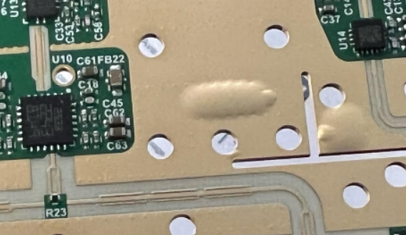
PCB blistering is primarily caused by defects in the electroless copper plating and electroplating processes during circuit board manufacturing, representing one of the most prevalent quality issues. The root cause of board surface blistering fundamentally stems from poor adhesion (interfacial bonding failure) or surface quality defects on the copper-plated layer.
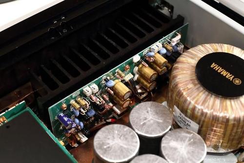
PCB (Printed Circuit Board) reliability test is crucial for ensuring the performance and durability of electronic devices. These tests are designed to evaluate the ability of PCBs to withstand various environmental and operational stressors over time. One of the key aspects of PCB reliability testing is thermal stress testing. This involves subjecting the PCB to extreme temperatures, both high and low, to simulate the conditions it may encounter in different applications. For example, a PCB in an automotive engine compartment may be exposed to high temperatures, while a PCB in an outdoor telecommunications equipment may experience extreme cold. By testing the PCB under these temperature extremes, potential weaknesses such as delamination, solder joint failures, and component degradation can be identified. Another important reliability test is mechanical stress testing. This includes vibration testing, shock testing, and bend testing. Vibration testing simulates the effects of mec
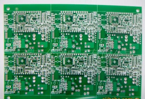
Manufacturing Process Precision Manufacturing Techniques High - frequency PCBA boards require highly precise manufacturing processes. The drilling of vias, which are used to connect different layers of the board, needs to be extremely accurate. The diameter of the vias and their placement must be within tight tolerances to avoid any impact on the signal integrity. Laser drilling is often used in the manufacturing of high - frequency PCBA boards as it can achieve very small via diameters with high precision. The soldering process also needs to be carefully controlled. In high - frequency applications, poor soldering joints can introduce impedance mismatches and signal reflections. Advanced soldering techniques, such as reflow soldering with precise temperature control, are used to ensure reliable and high - quality solder connections. For example, in the assembly of high - speed data transfer PCBA boards, the soldering of high - speed connectors and integrated circuits is crucial
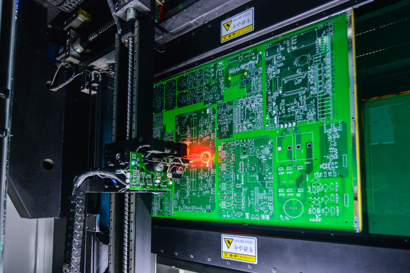
This article introduces several factors that affect the price of PCB.By understanding these factors, you can make more informed decisions when budgeting for PCB production.
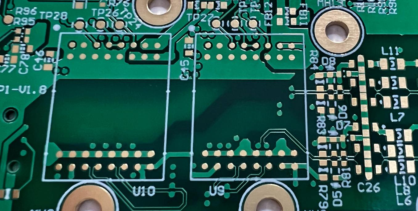
Understanding Vias holes (According to IPC-4761),Next, we will provide a introduction to Tent Via (Type I Via),Tented and Covered Via (Type II Via),Plugged Via (Type III Via),Plugged and Covered Via (Type IV Via),Filled Via (Type V Via),Filled and Covered Via (Type VI Via),Filled and Capped Via (Type VII Via).
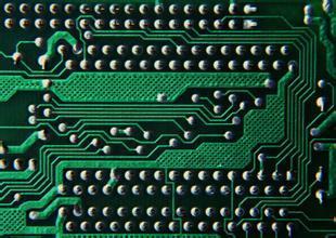
The price trend of PCBs (Printed Circuit Boards) is influenced by multiple factors, showing a complex and changeable situation. In recent years, the price of PCBs has generally trended upward. One of the main reasons is the fluctuation in raw material prices. PCBs mainly consist of copper foil, resin, glass fiber, and other materials. In the past few years, due to the booming lithium and new - energy automotive industries globally, the demand for copper has increased sharply, leading to a continuous rise in copper prices. As the main raw material of PCBs, the price increase of copper foil has directly driven up the production cost of PCBs. In addition, the prices of gold, silver, tin, and other precious metals, which are core components of PCBs, have also continued to rise, further increasing the cost of raw materials. Moreover, labor costs have been on the rise. With the improvement of living standards and the increase in labor protection requirements, the wage levels of workers
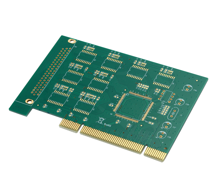
In the realm of modern electronics, PCB play a crucial role. They provide the physical and electrical infrastructure for connecting and supporting electronic components, allowing them to interact and function as intended. Without PCB, our electronic devices would be a chaotic mess of individual components with no way to communicate or work together.
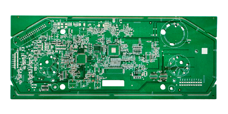
Introduction forThe Automotive Board and The Communication Board.
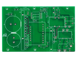
Flexible Printed Circuit Boards (PCBs) have revolutionized the electronics industry with their unique ability to bend, twist, and conform to various shapes. The materials used in the construction of flexible PCBs play a crucial role in determining their performance, flexibility, and durability. The base material of a flexible PCB is typically a polyimide (PI) film. Polyimide is highly regarded for its excellent thermal stability, high mechanical strength, and chemical resistance. It can withstand high temperatures, making it suitable for applications where the PCB may be exposed to heat, such as in automotive engine compartments or high - power electronics. The thermal stability of polyimide ensures that the flexible PCB does not deform or degrade under extreme temperature conditions, maintaining its electrical integrity. Additionally, its high mechanical strength allows the PCB to endure repeated bending and flexing without cracking or breaking. This is essential for applications
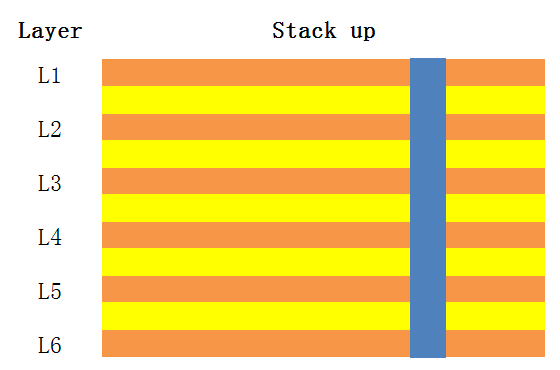
Via:A common type of hole is used for conducting or connecting copper foil lines between conductive patterns in different layers of a circuit board. But copper plated holes for component legs or other reinforcing materials cannot be inserted. Buried Hole:The connection between any circuit layer inside the PCB, but not conducting to the outer layer, also refers to the through-hole that does not extend to the surface of the circuit board. Blind Hole:Connecting the outermost circuit in the PCB with adjacent inner layers through plated holes is called blind pass because the opposite side cannot be seen. Blind holes are also conductive holes on one surface of the printed circuit board to increase the utilization of space between PCB circuit layers.
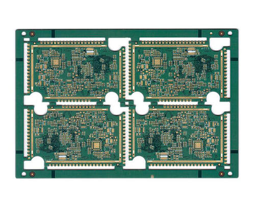
Preparation and Distribution of SMT Raw Materials In the SMT (Surface Mount Technology) process, the proper preparation and distribution of raw materials are fundamental steps that significantly impact the overall quality and efficiency of the production. The first aspect of raw material preparation is component procurement. High - quality electronic components, such as resistors, capacitors, integrated circuits (ICs), and inductors, need to be sourced from reliable suppliers. These components should meet strict specifications in terms of electrical properties, physical dimensions, and quality standards. For example, when procuring ICs, factors like the number of pins, pin pitch, and operating voltage range must be carefully considered to ensure compatibility with the circuit design. Once the components are received, they need to be properly stored. Components are often stored in a climate - controlled environment to prevent issues such as oxidation, moisture absorption, and physi
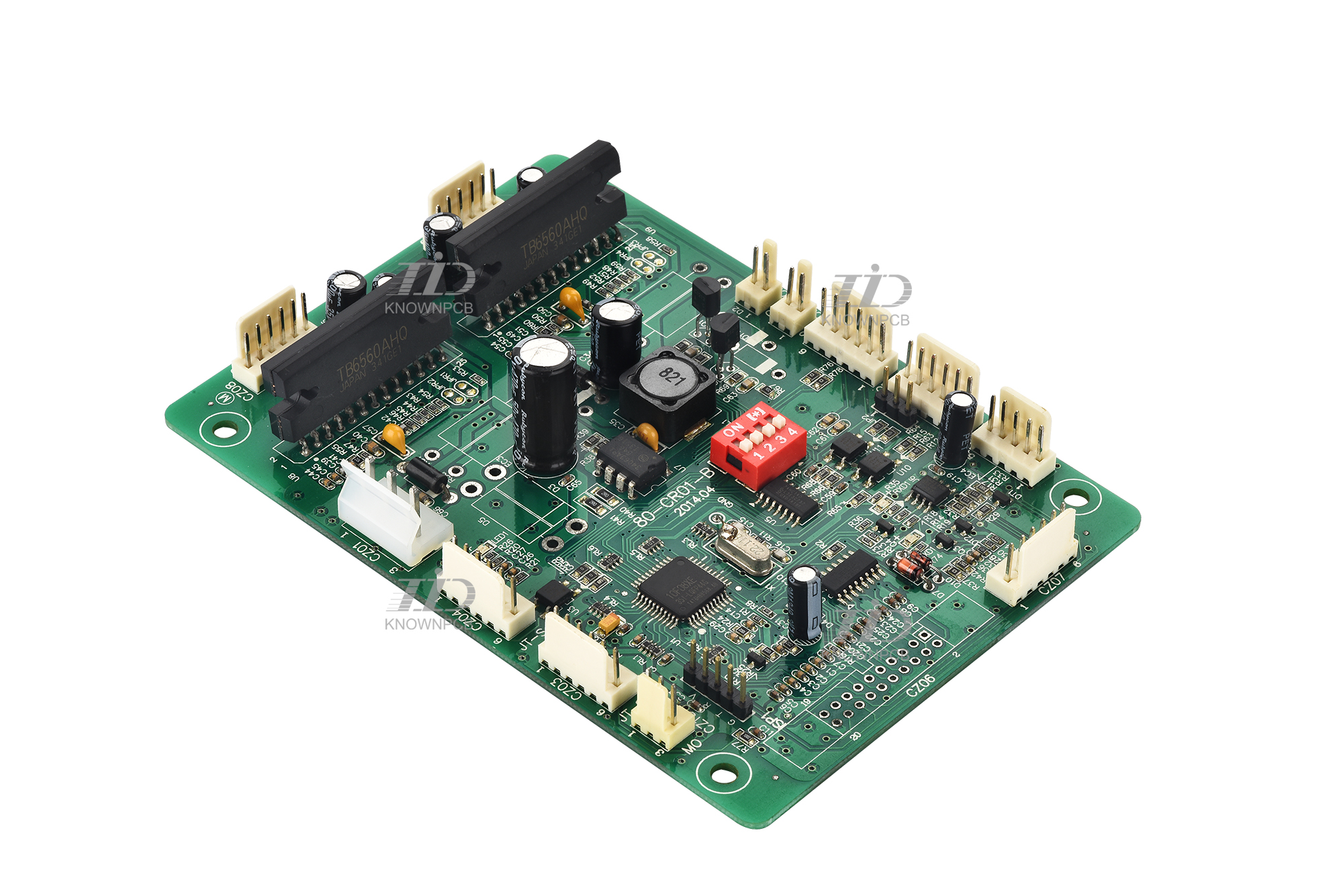
Introduce for Printed Circuit Board Assembly is to plug the SMT(Surface Mounted Technology) and the DIP in the Printed Circuit Board, also called PCBA.
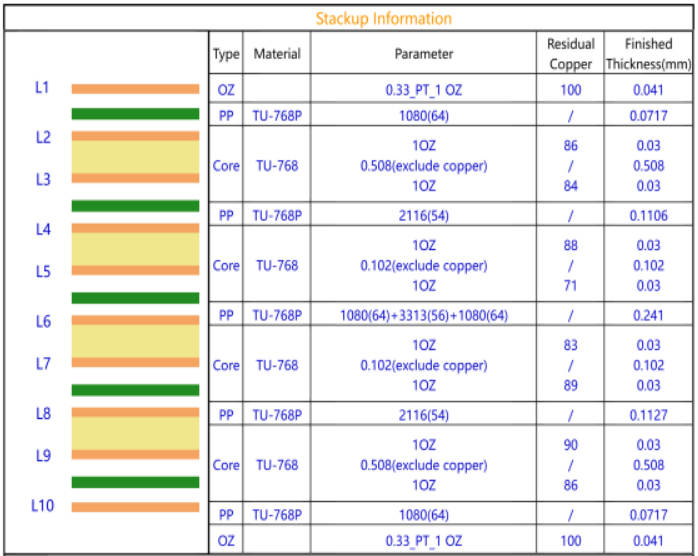
HDI board is different from ordinary PCB board materials. Nowadays, the difference is narrowing. The development of electronic products has led to wider application and faster development of HDI boards.

Structure Single layer board: A single layer PCB consists of only one layer of conductive material, usually copper, on one side of the insulating substrate. The other side is typically left uncoated or has only a solder mask or silk screen for markings. All the circuit traces, components, and connections are placed on this single conductive layer. It's like a one lane road where all the electrical signals have to travel in a single plane. Multilayer board: Multilayer PCBs, on the other hand, are composed of multiple layers of conductive material separated by insulating layers. These layers can include signal layers, power planes, and ground planes. For example, a 4 layer board might have two signal layers sandwiching a power plane and a ground plane. This structure is similar to a multi lane highway with different lanes dedicated to different types of traffic (electrical signals). Complexity of Circuit Design Single layer board: Due to the limited space and the need to rout

Flexible Printed Circuit Boards (FPCB/FPC) are crucial in modern electronics. FPCB have different structures. Single - layer ones have a substrate with copper foil and cover layers bonded by adhesive. Double - layer FPCs have copper foil on the substrate, fixed in different ways, and additional outer layers. Multi - layer FPCs are stacked single - or double - layer FPCs. FPC stacking involves considering layer details for flexibility. Due to features like flexibility, thinness, and high - density circuits, FPCBs are used in commercial electronics, communication, military, aerospace, and medical equipment.
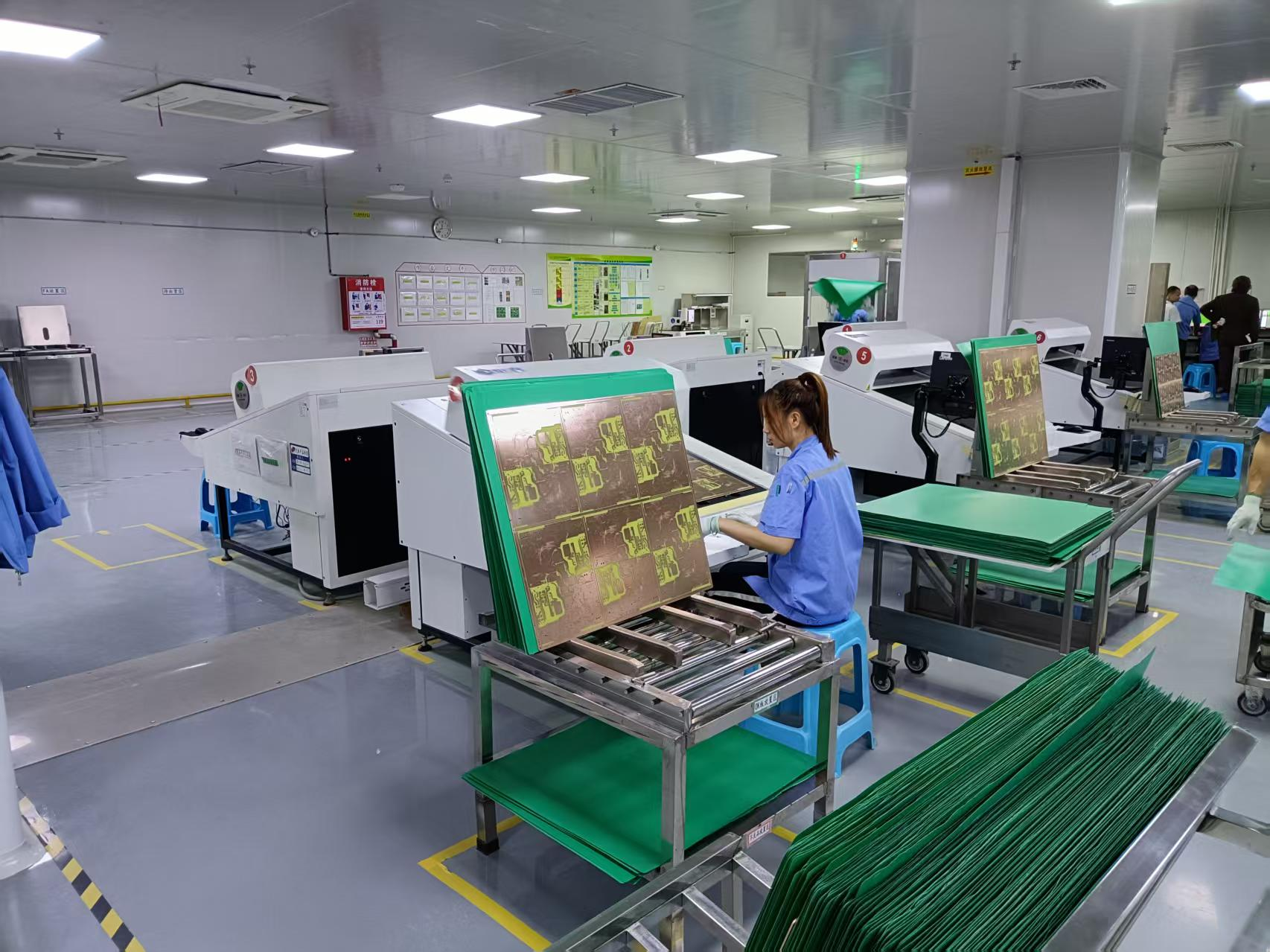
Halogen-free PCBs are environmentally friendly, made from substrates processed without halogens like chlorine or bromine. These materials are replaced or reduced to meet halogen-free standards, often requiring special design considerations. Most halogen-free boards use phosphorus and phosphorus-nitrogen compounds, which form a carbonized film during combustion, isolating the resin from air and enhancing flame retardancy.
Inquiry Now

