 +86 755 2794 4155
  sales@knownpcb.com
-
Shenzhen KNOWNPCB Technology Co., Ltd.
 +86 755 2794 4155
  sales@knownpcb.com
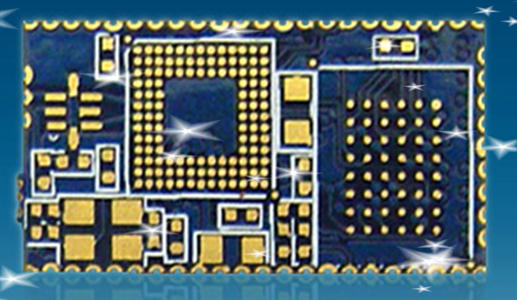
Printed Circuit Boards (PCBs) are an essential component of many electronic devices. However, like any complex system, PCBs can experience problems that require troubleshooting. Here are some common PCB troubleshooting methods: 1. Visual Inspection: The first step in troubleshooting a PCB is to perform a visual inspection. Look for signs of damage such as burned components, broken traces, or loose connections. Check for any obvious signs of physical damage that could be causing the problem. 2. Power Supply Check: Check the power supply to the PCB. Make sure that the correct voltage and current are being supplied. Use a multimeter to measure the voltage at different points on the PCB to ensure that the power is reaching all the components. 3. Component Testing: Test individual components on the PCB to determine if they are functioning properly. Use a multimeter or an oscilloscope to test for continuity, resistance, and capacitance. Replace any faulty components as needed. 4. Sig
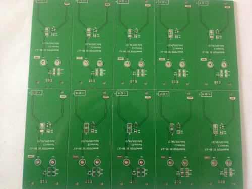
As the demand for electronic devices continues to grow, so does the concern for the environmental impact of printed circuit boards (PCBs). PCBs contain a variety of materials that can be harmful to the environment if not properly disposed of or recycled. Here are some environmental solutions for PCBs: 1. Design for Environment (DfE): Incorporate environmental considerations into the design of PCBs. This includes using materials that are less harmful to the environment, reducing the use of hazardous substances, and designing for recyclability. For example, use lead-free solder and halogen-free materials. 2. Recycling: Implement a recycling program for PCBs. This can involve collecting used PCBs and sending them to a recycling facility where the materials can be recovered and reused. Recycling PCBs can reduce the amount of waste sent to landfills and conserve natural resources. 3. Waste Reduction: Minimize waste generated during the manufacturing process of PCBs. This can be achie
Printed Circuit Boards (PCBs) are a critical component of many electronic devices, but they can also be a significant cost factor. Here are some methods for controlling the cost of PCBs: 1. Design Optimization: Optimize the PCB design to reduce costs. This can include reducing the number of layers, minimizing the board size, and using standard components. Avoid over-designing the PCB and focus on meeting the functional requirements while keeping costs down. 2. Material Selection: Choose cost-effective materials for the PCB. Consider using alternative materials that offer similar performance but at a lower cost. For example, use FR-4 instead of more expensive high-performance materials. Also, consider using surface mount technology (SMT) components instead of through-hole components, as SMT components are generally cheaper. 3. Volume Production: Produce PCBs in large volumes to take advantage of economies of scale. Negotiate with suppliers for better prices based on volume orders
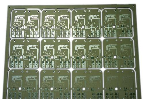
Quality control is essential for ensuring the reliability and performance of printed circuit boards (PCBs). Here are some key points to consider for PCB quality control: 1. Design Review: Conduct a thorough design review before manufacturing the PCB. Check for design errors, compatibility issues, and potential manufacturing problems. Ensure that the design meets the required specifications and standards. 2. Material Inspection: Inspect the materials used for PCB manufacturing, such as copper foil, laminate, and components. Ensure that the materials are of high quality and meet the required specifications. Check for any defects or contaminants that could affect the quality of the PCB. 3. Manufacturing Process Control: Monitor and control the manufacturing process to ensure consistent quality. This includes processes such as etching, plating, drilling, and soldering. Use quality control tools and techniques such as statistical process control (SPC) to detect and correct any proces
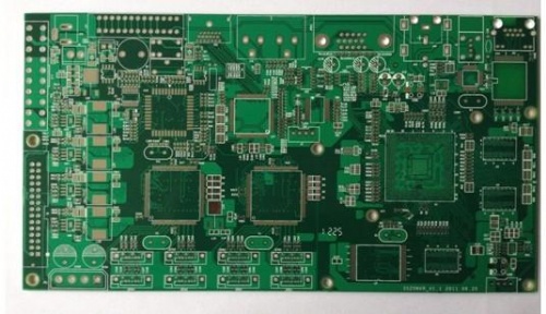
In today's complex electronic systems, high reliability printed circuit boards (PCBs) are essential. A high reliability PCB is designed and manufactured to ensure consistent performance and durability even in demanding environments. One of the key factors in achieving high reliability is the selection of quality materials. Premium-grade substrates, copper foils, and soldermasks are used to ensure excellent electrical insulation, thermal conductivity, and mechanical strength. These materials are carefully chosen to withstand temperature variations, humidity, and mechanical stress. The design process also plays a crucial role. Engineers use advanced design software and follow strict design guidelines to optimize the layout for signal integrity, power distribution, and thermal management. This includes minimizing signal interference, providing proper grounding, and ensuring efficient heat dissipation. Manufacturing processes are equally important. High reliability PCBs are typicall

High - speed signal integrity PCBs are essential in today's high - performance electronic systems where data transfer speeds are constantly increasing. The first key aspect in high - speed signal integrity PCBs is impedance control. As the speed of signals increases, any impedance mismatch can lead to significant signal reflections. The PCB traces are designed with specific impedance values, usually 50 ohms or 75 ohms depending on the application. This requires precise control of the trace width, thickness, and the dielectric constant of the substrate material. For example, in a high - speed communication PCB, the impedance of the transmission lines must be carefully matched to the input and output impedance of the connected components such as high - speed transceivers. Another important factor is the reduction of signal crosstalk. At high speeds, electromagnetic fields around the traces can couple with adjacent traces, causing interference. To minimize crosstalk, designers use t
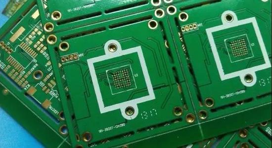
Ultra thin PCBs have unique specifications that make them highly suitable for specific applications where space and flexibility are of utmost importance. The thickness of an ultra thin PCB is one of its most defining characteristics. Typically, these PCBs can have a thickness ranging from as little as 0.1mm to a few tenths of a millimeter. This extremely thin profile allows them to be used in applications where space is severely limited. For example, in modern smartphones and tablets, ultra thin PCBs enable the device manufacturers to make the products thinner and more compact. They can be easily integrated into the slim body of the device without adding significant bulk. The materials used in ultra thin PCBs are carefully selected. Special substrate materials are often employed that have both good electrical properties and the required mechanical strength at such thin dimensions. For instance, flexible materials like polyimide are commonly used. Polyimide based substrates offer
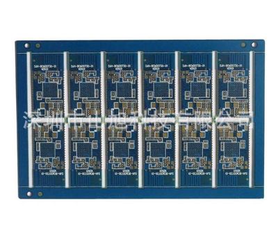
There are various ways to split PCB boards, and the following will introduce several common ways of splitting: 1. Milling and cutting of PCB boards: Using a CNC milling machine, cut grooves on the PCB board and use a rotating tool or milling cutter to cut the board into small pieces, suitable for various shapes and sizes of boards. 2. Punching and Splitting: Through die-cutting technology, holes are pressed on the PCB board, and then force is applied to break the board, achieving the splitting operation, suitable for rectangular and regular shaped boards. 3. V-knife board splitting: Use a special V-shaped blade to cut V-shaped slots on the PCB board, then apply force to break the board and separate it into small pieces, suitable for thinner boards and situations with high precision requirements. 4. Laser board splitting: Using laser cutting technology, precise cutting can be performed on PCB boards to achieve complex shapes and high-precision board splitting requirements, suita
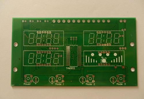
Printed Circuit Boards (PCBs) are essential components in electronic devices, and anti - oxidation treatment of PCBs is of great significance to ensure their long - term performance and reliability. The main purpose of PCB anti - oxidation treatment is to prevent the copper surfaces on the PCB from oxidizing. Copper is widely used in PCBs for its excellent electrical conductivity. However, copper is highly susceptible to oxidation when exposed to air, moisture, and other environmental factors. Oxidation of copper can form copper oxide or other copper compounds, which can increase the resistance of the circuit, degrade the electrical performance of the PCB, and even lead to potential failure of the entire electronic system. There are several common methods for PCB anti - oxidation treatment. One of the most widely used techniques is the application of anti - oxidation coatings. These coatings can be organic or inorganic materials. Organic coatings usually contain polymers with cer
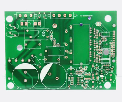
Specific size PCB A specific size PCB (Printed Circuit Board) plays a crucial role in various electronic devices, and its design and manufacturing are carefully tailored to meet specific requirements. When dealing with a specific size PCB, the first consideration is the physical dimensions. These dimensions are determined by the available space within the device it will be installed in. For example, in a handheld consumer electronics device like a smartwatch, the PCB size is extremely limited. It needs to fit within the tiny casing while accommodating all the necessary components such as the microprocessor, memory chips, sensors, and connectivity modules. In contrast, in a larger device like a desktop computer motherboard, the PCB size can be much larger to provide enough space for numerous components, expansion slots, and connectors. The size also affects the routing of the traces on the PCB. In a small size PCB, the traces need to be carefully designed to avoid short circuits an
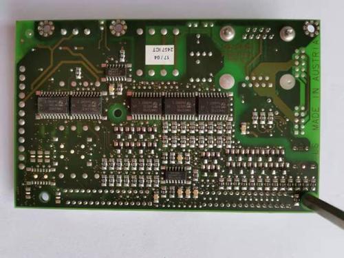
High - thermal - conductivity printed circuit boards (PCBs) play a crucial role in electronic devices where efficient heat dissipation is essential. These PCBs are designed to manage heat effectively, thereby improving the reliability and performance of the overall system. The materials used in high - thermal - conductivity PCBs are the key to their heat - dissipating capabilities. One common approach is to use metal - based substrates. For example, aluminum - based PCBs are widely used. The aluminum core provides an excellent heat - conducting path. The copper layers on the PCB are laminated onto the aluminum substrate, allowing heat generated by the components to be quickly transferred to the aluminum and then dissipated into the surrounding environment. Another option is to use ceramic - based materials. Ceramic substrates have high thermal conductivity and can withstand high temperatures. They are often used in high - power applications such as power amplifiers and LED lightin
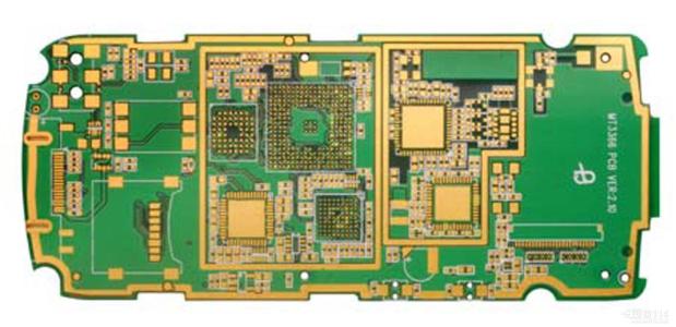
1. Introduction to PCB Industry Standards The printed circuit board (PCB) industry is highly regulated by a set of standards that ensure the quality, reliability, and compatibility of PCBs in various applications. These standards are developed by international organizations, industry associations, and regulatory bodies. 2. Design and Layout Standards Component Placement and Spacing One of the key aspects of PCB design standards is component placement and spacing. There are specific rules regarding how close components can be placed to each other. For example, to prevent short - circuits and ensure proper heat dissipation, there are minimum distances specified between different types of components. Surface - mount components may have different spacing requirements compared to through - hole components. In addition, the orientation of components is also standardized in some cases. This is to ensure consistent manufacturing processes and ease of inspection. For example, polarized
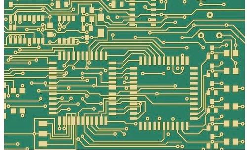
PCB board materials are classified based on several factors, including their performance characteristics, intended applications, and manufacturing requirements. 1. Based on Substrate Materials One of the main ways to classify PCB materials is by the type of substrate used. The most common substrate material is fiberglass reinforced epoxy resin, known as FR 4. FR 4 boards have good mechanical strength, electrical insulation properties, and are suitable for a wide range of applications. They can withstand relatively high temperatures during the soldering process and have stable dielectric properties. Another type of substrate is polyimide, which is used in high temperature and high frequency applications. Polyimide based PCBs can operate at much higher temperatures than FR 4 boards and have excellent dielectric properties at high frequencies. They are often used in aerospace, military, and some high end electronics applications where temperature and frequency stability are crucial.

A high-capacity energy storage power source is essential in various applications where a large amount of energy needs to be stored and supplied reliably. One of the key areas where it is highly valuable is in off-grid power systems. For example, in remote areas where access to the main power grid is limited or unavailable, such as mountain cabins or rural villages, a high-capacity energy storage power source can store energy from renewable sources like solar panels or wind turbines. This stored energy can then be used to power electrical appliances, lighting, and other essential equipment throughout the day and night. In the event of bad weather or low renewable energy generation, the large energy storage capacity ensures that there is still a sufficient supply of power to meet the basic needs. Another application is in emergency backup power systems. During power outages caused by natural disasters, grid failures, or other unforeseen circumstances, a high-capacity energy storage
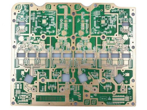
PCB (Printed Circuit Board) board welding is a critical process in electronics manufacturing, and there are several national standards in place to ensure the quality and reliability of the soldered connections. 1. Soldering Material Standards The choice of soldering materials, such as solder paste and solder wire, is governed by specific standards. For solder paste, its composition, including the ratio of tin, lead (in lead containing solders), and other alloying elements, is precisely defined. The viscosity of the solder paste is also a crucial parameter as it affects the printing accuracy and the ability to hold components in place during reflow soldering. In the case of solder wire, its diameter and the content of flux are standardized. Flux helps in cleaning the metal surfaces to be soldered and promotes the wetting of the solder, ensuring a good bond. The flux content and its activity level are specified to meet different soldering requirements, such as for through hole comp
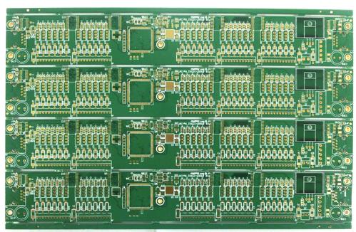
A power electronic PCB (Printed Circuit Board) is a crucial component in various electrical and electronic systems that deal with the control and conversion of electrical power. It is designed to handle high voltages and currents, making it essential for applications such as power supplies, motor drives, and renewable energy systems. The design of a power electronic PCB requires careful consideration of several factors. One of the key aspects is the layout. The components on the PCB need to be arranged in a way that minimizes the length of the power traces to reduce resistance and inductance. This is crucial as it helps in minimizing power losses and improving the efficiency of the power conversion process. For example, in a power supply PCB, the placement of the capacitors, inductors, and power transistors is carefully planned to ensure smooth flow of current and voltage. Another important consideration is the thermal management. Power electronic components generate a significan

High-precision printed circuit boards (PCBs) are essential for applications that demand exceptional electrical performance and reliability. These PCBs require strict specification requirements to ensure accurate and consistent functionality. One of the key requirements for high-precision PCBs is tight dimensional tolerance. The board dimensions, hole locations, and trace widths and spacings must be controlled within very narrow limits to ensure proper component placement and signal integrity. This often requires advanced manufacturing processes and precision machinery. High-precision PCBs also require excellent surface finish. The copper surfaces must be smooth and free from defects to ensure good solderability and electrical conductivity. Common surface finishes for high-precision PCBs include immersion gold, electroless nickel/immersion gold (ENIG), and organic solderability preservative (OSP). Signal integrity is another critical aspect of high-precision PCBs. The traces must
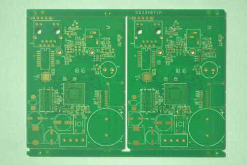
Printed Circuit Boards (PCBs) with standard specifications play a crucial role in various electronic applications. These PCBs are designed to meet common industry requirements and offer reliable performance. The standard specification PCB typically consists of a rigid or flexible substrate material, such as FR-4 glass epoxy or polyimide. The substrate provides mechanical support and electrical insulation for the components and traces on the board. The copper traces on a standard PCB are laid out according to the circuit design, connecting the various components such as resistors, capacitors, integrated circuits, and connectors. The trace width and spacing are usually determined based on the current-carrying capacity and signal integrity requirements. Standard PCBs often have a defined number of layers, ranging from single-sided to multilayer configurations. Single-sided PCBs have components and traces on one side only, while double-sided PCBs have components and traces on both s

The PCB fixture test is a common method used to test the functionality and quality of printed circuit boards (PCBs). This test involves using a custom-made fixture that holds the PCB in place and provides electrical connections for testing. The fixture is designed to fit the specific dimensions and layout of the PCB being tested. It typically consists of a base plate, a set of alignment pins, and a series of spring-loaded probes or contacts. The alignment pins ensure that the PCB is properly positioned in the fixture, while the probes or contacts make electrical connections to the PCB's test points. Once the PCB is inserted into the fixture, the test equipment is connected to the fixture's electrical contacts. The test equipment then applies various electrical signals and measurements to the PCB to determine if it is functioning properly. This may include testing for continuity, resistance, capacitance, and other electrical parameters. One of the main advantages of the PCB fixtu
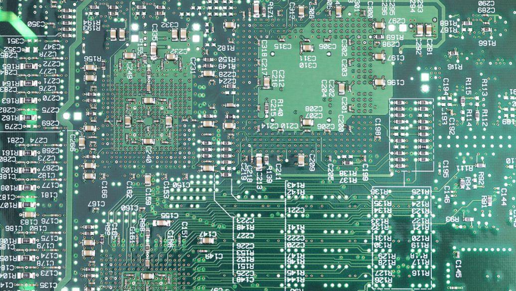
The PCB flying probe test is a method used to test the electrical functionality of printed circuit boards (PCBs). This test is performed using specialized equipment that consists of multiple probes that can move independently and make contact with the PCB at different points. The flying probe test works by sending electrical signals through the PCB and measuring the responses at various points. The probes are programmed to move to specific locations on the PCB and make contact with the conductive traces or pads. The test equipment then applies electrical stimuli, such as voltage or current, and measures the resulting responses, such as resistance, capacitance, or inductance. One of the main advantages of the flying probe test is its flexibility. Since the probes can move independently, they can test PCBs of different sizes and shapes without the need for custom fixtures or test jigs. This makes the flying probe test ideal for small-volume production runs or for testing prototypes
Inquiry Now

