 +86 755 2794 4155
  sales@knownpcb.com
-
Shenzhen KNOWNPCB Technology Co., Ltd.
 +86 755 2794 4155
  sales@knownpcb.com
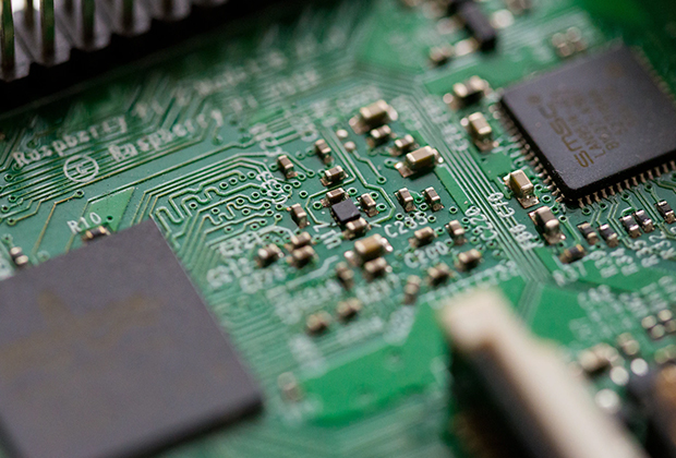
Have you noticed that now more and more of our lighting is using led lighting.What is LED? Compared to the traditional light bulbs, LEDs have lower power consumption, longer lifetime and higher energy efficiency. In the PCB industry,when we say LED PCB, it refers to the pcb used for LED lighting, if you are looking for a suitable LED PCB for your lighting system, this article may bring you something. WHAT ARE LEDS COMPOSED OF?LED is an initial light-emitting diode that produces light when an electric current passes through. LEDs typically have negative and positive electrodes, which generate light in the visible light region.The LEDS are glued to the PCB by soldering process and have electrical connections for lighting.Since light-emitting diodes dissipate a lot of heat when they are in use, when you are designing LED, the metal core is usually the best choice for LED PCB, it is because that it dissipates heat more faster. Among them, the metal material aluminum is the most widely used
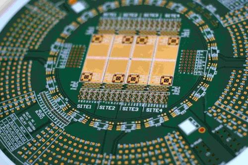
With the increasing global awareness of environmental protection, ROHS (Restriction of Hazardous Substances) standards have become an important norm in the electronics industry. Our company actively responds to the call for environmental protection and has launched printed circuit boards (ROHS PCBs) that comply with ROHS standards. These circuit boards not only have excellent electrical performance, but also strictly limit the use of harmful substances to ensure minimal impact on the environment. Our ROHS printed circuit board uses lead-free solder, halogen-free materials, and low pollution chemical treatment processes. In the production process, we strictly comply with environmental regulations and reduce environmental pollution through advanced waste treatment systems and resource recycling technologies. In addition, we have also obtained multiple international environmental certifications to ensure that the environmental performance of our products reaches the international adv
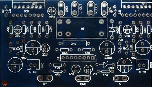
Printed Circuit Board (PCB) is an essential core component in modern electronic products. It connects various electronic components such as resistors, capacitors, transistors, etc. by printing conductive patterns on an insulating substrate to achieve circuit functionality and signal transmission. The application range of PCB is extremely wide, from household appliances to aerospace equipment, almost all electronic devices cannot do without its support. The main advantage of PCB lies in its high-density integration and automated production. Through multi-layer stacking and precision machining techniques, complex circuit designs can be achieved in limited space, greatly improving the performance and reliability of electronic devices. In addition, the standardized production and testing process of PCBs ensures high quality and consistency of products, reducing manufacturing costs and cycles. During the design and manufacturing process, engineers use professional EDA software for cir
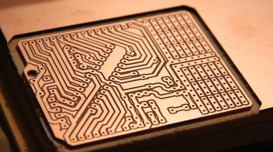
Printed Circuit Board (PCB) is the heart and nerve center of modern electronic products. It achieves electrical connection and signal transmission between electronic components by printing conductive circuits on insulating substrates. The widespread application and importance of printed circuit boards (PCBs) make them the foundation and core of modern electronics industry. The main functions of a printed circuit board (PCB) include electrical connections, signal transmission, and component support. By installing various electronic components such as resistors, capacitors, transistors, and integrated circuits on circuit boards, electronic products can achieve complex functions and efficient operation. The manufacturing process of printed circuit boards (PCBs) is very complex, including multiple steps such as circuit design, substrate selection, copper foil etching, drilling, and surface treatment. Each step requires strict quality control and precise process technology. With the c
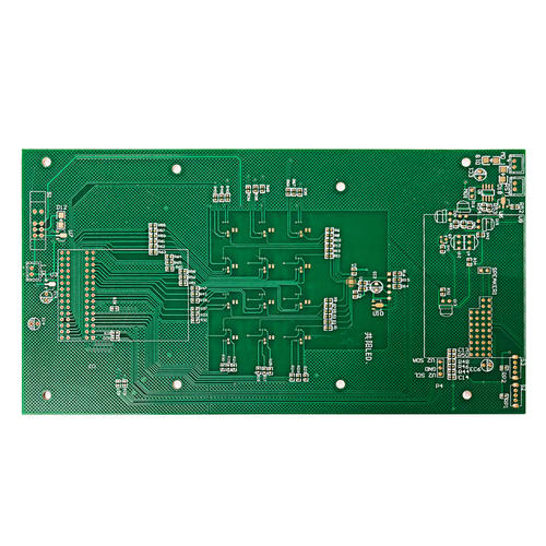
Printed circuit boards (PCBs) are an indispensable part of modern electronic devices, and copper plays a crucial role in them. Copper circuit board, as the name suggests, is a circuit board that uses copper as a conductive material. Copper, due to its excellent conductivity and ductility, has become an ideal choice for making circuit boards. During the manufacturing process, copper is plated on a substrate and then circuit patterns are formed through photolithography and etching processes. These copper wires are responsible for connecting various electronic components, allowing the current to flow smoothly. The high conductivity of copper means that circuit boards can achieve efficient electrical connections in a small space, thereby reducing resistance and energy loss. In addition, copper also has good corrosion resistance and oxidation resistance, which enables copper circuit boards to maintain stable performance in various harsh environments. Copper can ensure the long-term re
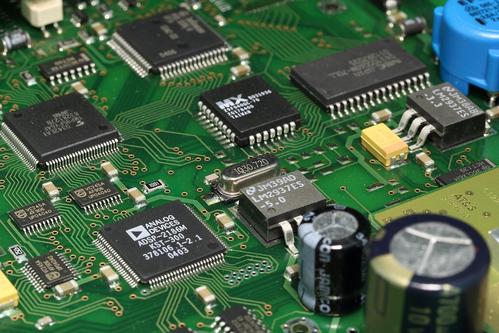
Copper plated circuit board is a circuit board that is coated with a layer of copper on a substrate to form a circuit pattern. Copper plating process is one of the key steps in manufacturing PCBs, which forms fine circuit patterns on the substrate to achieve electrical connections between electronic components. In the copper plating process, electroplating or chemical plating methods are usually used. Electroplating is the process of depositing copper ions onto a substrate through an electrolytic cell, while chemical plating utilizes chemical reactions to form a copper layer on the surface of the substrate. Regardless of the method, precise control of process parameters is required to ensure the uniformity of the copper layer and the accuracy of the circuit. Copper plated circuit boards are widely used in various electronic devices, including computers, communication equipment, consumer electronics products, and automotive electronic systems. Its superior conductivity and mechani
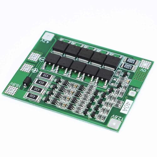
Copper clad circuit boards, as an indispensable basic material in modern electronic industry, are widely used in various electronic and communication equipment. Copper clad circuit board, as the name suggests, is a circuit board made by covering a layer of copper foil on the substrate and using a series of processes such as etching, drilling, and copper plating. It is not only the support for electronic components, but also the carrier for electrical connections of electronic components. The main materials of copper-clad circuit boards include substrates, copper foil, and adhesives. The substrate is usually made of glass fiber reinforced epoxy resin board, which has good insulation and heat resistance. Copper foil is used as a conductive material to create circuit patterns. Adhesive is used to bond copper foil and substrate together, ensuring the mechanical strength and electrical performance of the circuit board. The key performance indicators of copper-clad circuit boards inclu
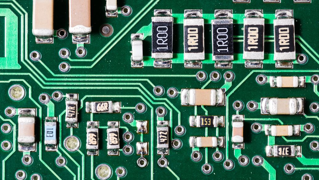
Copper circuit boards, with their excellent conductivity and mechanical properties, have become an indispensable basic material in modern electronic industry. Copper circuit boards are widely used in various electronic and communication devices, playing an important role in supporting electronic components and achieving electrical connections. The main materials of copper circuit boards include copper foil, substrate, and adhesive. Copper foil, as a conductive material, is used to make circuit patterns. The substrate serves as the support body and is usually made of glass fiber reinforced epoxy resin board, which has good insulation and heat resistance. Adhesive is used to bond copper foil and substrate together, ensuring the mechanical strength and electrical performance of the circuit board. The key performance indicators of copper circuit boards include heat resistance, chemical resistance, dielectric constant, and mechanical strength. These indicators directly affect the reli
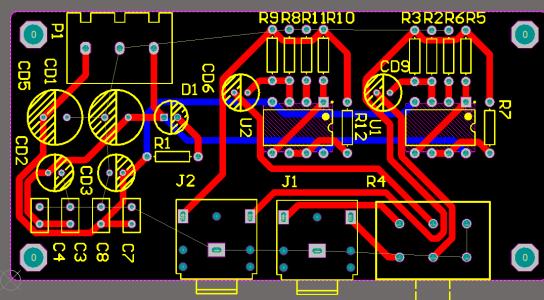
Printed Circuit Board (PCB), as the core component of modern electronic devices, is almost ubiquitous. From smartphones and tablets to cars and household appliances, PCBs play a crucial role in various fields. It not only carries various electronic components, but also is responsible for the electrical connection between them to ensure the normal operation of the equipment. The basic structure of copper-clad circuit boards consists of one or more copper foil layers and non-conductive substrates. The copper foil layer forms complex circuit patterns through etching technology, including wires, solder pads, and through holes. Non conductive substrates typically use glass fiber, epoxy resin, or other composite materials to provide mechanical support and insulation performance. As needed, PCBs can be designed as single-layer, double-layer, or multi-layer structures to meet the functional requirements and space limitations of different electronic devices. During the manufacturing proce
Inquiry Now

