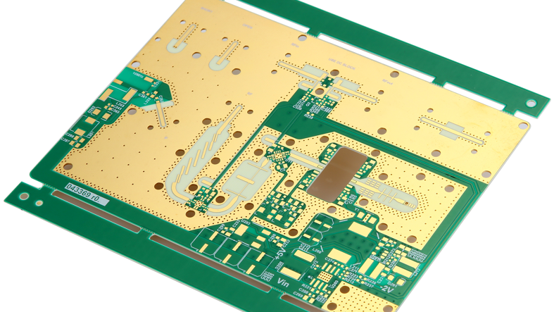
High Frequency / High-Speed PCBs High frequency and high-speed PCBs are specialized circuit boards designed to handle signals with high frequencies and fast data rates. Applications of High Frequency / High-Speed PCBs 1. Telecommunications: - RF and Microwave Circuits: Used in antennas, transceivers, and other RF components in telecom infrastructure. - 5G Technology: Essential for high-frequency signal processing in 5G base stations and devices. 2. Computing and Networking: - High-Speed Data Processing: Applied in servers, data centers, and network switches requiring fast data transmission and processing. - PCI Express and High-Speed Interfaces: Utilized in PCBs for high-speed interfaces such as PCIe, USB 3.0, and HDMI. 3. Automotive and Aerospace: - Advanced Driver Assistance Systems (ADAS): Used in radar, LiDAR, and other sensor systems for high-frequency signal processing. - Avionics: Essential for high-speed communication and data processing systems in aircraft. 4. Medical Devices: - Imaging Equipment: Applied in MRI and CT scanners where high-frequency signals are used for imaging and diagnostics. - Patient Monitoring Systems: Used in high-speed data acquisition and processing for real-time monitoring. Features of High Frequency / High-Speed PCBs 1. Material Selection: - Low-Loss Dielectric Materials: Use of materials such as Rogers, Teflon (PTFE), FR4 High-Speed, and other advanced laminates that offer low dielectric loss and stable dielectric constant (Dk). - Controlled Impedance: Ensures signal integrity by maintaining consistent impedance across traces, crucial for high-speed signal transmission. 2. Design Techniques: - Microstrip and Stripline: Techniques for routing high-frequency signals on outer and inner layers respectively to control impedance and minimize signal loss. - Differential Pairs: Use of differential signaling for high-speed data lines to reduce electromagnetic interference (EMI) and crosstalk. - Via Design: Optimized via structures, such as back-drilled vias and blind/buried vias, to reduce signal reflection and improve performance. 3. Signal Integrity: - Minimized Crosstalk: Careful routing and layer stack-up design to reduce interference between adjacent traces. - Low Signal Attenuation: Ensures signals maintain their integrity over long distances by using high-quality materials and proper trace design. 4. Thermal Management: - Effective Heat Dissipation: High-speed and high-frequency PCBs often generate significant heat, requiring advanced thermal management solutions like heat sinks, thermal vias, and proper ventilation. High frequency and high-speed PCBs are critical for applications requiring fast data rates and reliable signal integrity, such as telecommunications, computing, automotive, aerospace, and medical devices. They feature low-loss dielectric materials, controlled impedance design, and advanced layout techniques to ensure optimal performance. Contact us for expert assistance and a one-stop solution for your high-frequency and high-speed PCB needs.(We have more than 15 years of production and overseas PCB experience) |  +86 755 2794 4155
  sales@knownpcb.com

 EN
EN CN
CN 中文
中文 Home >