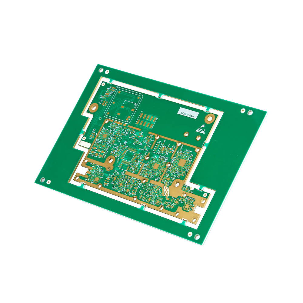
Key Features and Benefits
Enhanced Power Distribution: The power plane design ensures efficient and stable power distribution across the PCB, minimizing voltage drops and providing consistent power to all components.
Reduced EMI and Noise: Incorporates a dedicated power plane that helps to reduce electromagnetic interference (EMI) and noise, improving overall signal integrity and performance.
Thermal Management: Features optimized thermal pathways that enhance heat dissipation, preventing overheating and ensuring reliable operation of high-power components.
High Current Capacity: Capable of handling high current loads, making it suitable for applications requiring robust power delivery.
Improved Signal Integrity: The use of multiple layers allows for better signal routing and isolation, reducing crosstalk and enhancing signal integrity.
Compact Design: The multi-layer structure enables more compact and densely populated PCB designs, saving space and allowing for more complex circuitry.
Versatility: Suitable for a wide range of applications, including consumer electronics, industrial equipment, automotive systems, and more.
Durable Construction: Made with high-quality materials and manufacturing processes, ensuring long-term reliability and durability.
Cost-Effective: Offers a balance between performance and cost, providing a reliable power distribution solution without significantly increasing manufacturing costs.
Customization Options
Layer Count: Choose between 2-layer and 4-layer configurations depending on the complexity and power requirements of your application.
Material Selection: Options to select different PCB materials such as FR4, high-temperature laminates, or other specialized materials based on specific needs.
Copper Thickness: Customize the copper thickness to handle varying current loads, with options for standard or heavy copper layers.
Power Plane Configuration: Tailor the power plane layout to suit your specific power distribution needs, including the placement and routing of power and ground planes.
Thermal Vias: Add thermal vias to enhance heat dissipation in high-power areas, improving the thermal management capabilities of the PCB.
Impedance Control: Implement impedance control features for high-speed signal integrity, ensuring optimal performance in high-frequency applications.
Surface Finish: Choose from a variety of surface finishes, including HASL, ENIG, OSP, and more, to meet your assembly and environmental requirements.
Solder Mask and Silkscreen: Customize the color and design of the solder mask and silkscreen to meet aesthetic or branding requirements.
Component Placement: Specify custom component placement and routing to optimize the layout for your particular design and application.
Testing and Certification: Request additional testing and certification services, such as IPC standards compliance, to ensure the highest quality and reliability.
Prototyping and Production Runs: Options for small-scale prototyping as well as full-scale production runs, allowing you to scale your project as needed.
 +86 755 2794 4155
  sales@knownpcb.com

 EN
EN CN
CN 中文
中文

 Home >