Product Overview
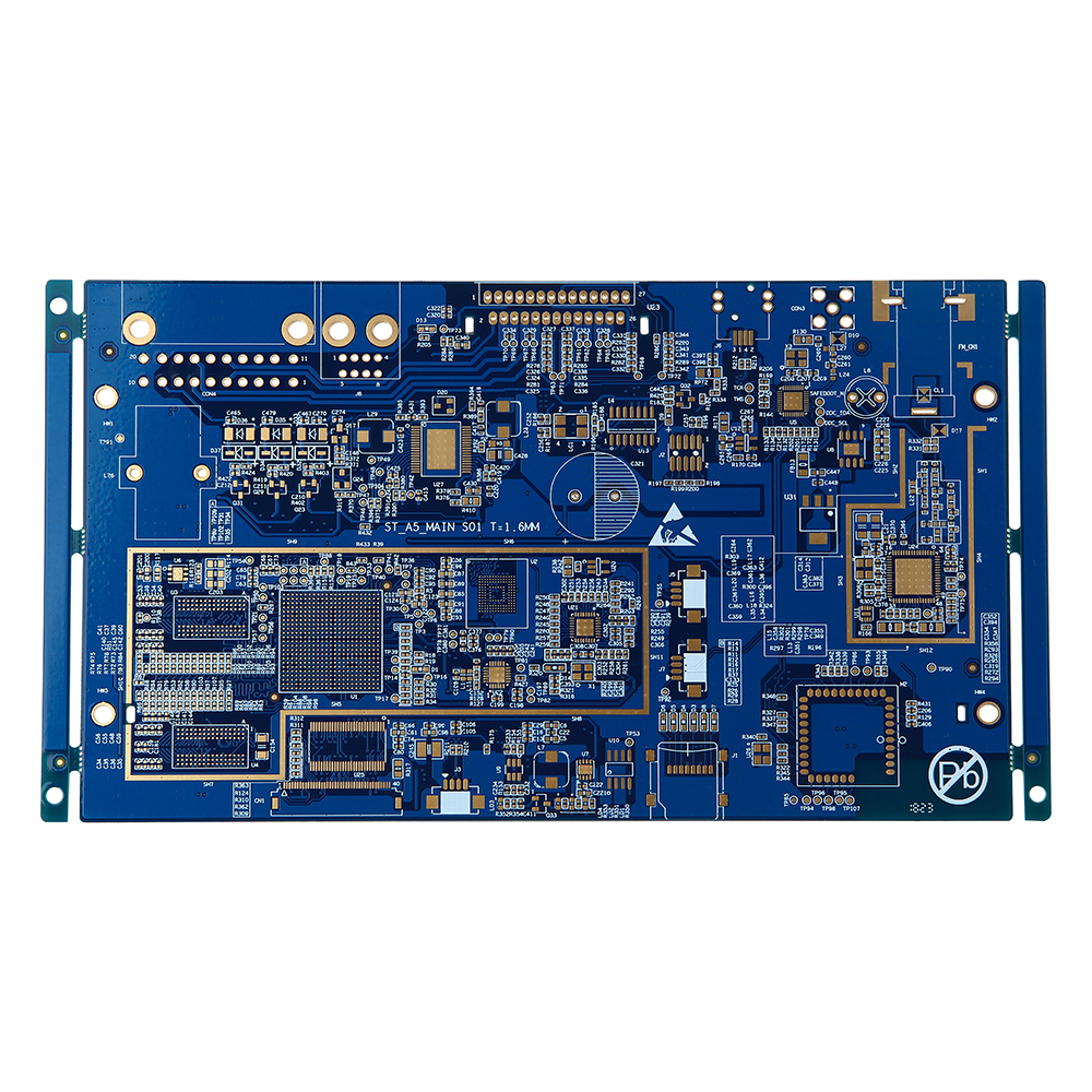
PCB Reverse Engineering is a specialized service aimed at analyzing and reconstructing existing printed circuit boards (PCBs) to understand their design, functionality, and components. This process involves creating accurate schematics and layout files from a physical PCB, which can then be used for troubleshooting, redesign, or replication. Our PCB Reverse Engineering service is essential for situations where original design files are unavailable or lost, and it provides a cost-effective solution for maintaining and updating legacy systems.
Key Features:
Accurate Reconstruction: Precise replication of PCB schematics and layout.
Component Identification: Detailed analysis and identification of all components.
Documentation: Comprehensive documentation including schematics, bill of materials (BOM), and Gerber files.
Troubleshooting and Repair: Assists in diagnosing issues and repairing faulty boards.
Customization: Ability to modify and improve the original design based on current requirements.
Legacy Support: Essential for maintaining and updating older systems where original documentation is not available.
Technical Details
1. Reverse Engineering Process:
Initial Assessment: Visual inspection and preliminary analysis of the PCB.
Imaging and Scanning: High-resolution imaging and scanning of the PCB to capture all details.
Layer Separation: Careful separation and analysis of each PCB layer to understand the layout and connections.
Schematic Capture: Recreating the original circuit schematic based on the physical board and connections.
Layout Recreation: Reconstructing the PCB layout using advanced CAD software to produce accurate design files.
2. Component Analysis:
Identification: Detailed identification of all components including resistors, capacitors, ICs, and connectors.
Value Extraction: Determination of component values and specifications.
BOM Generation: Creation of a complete bill of materials listing all components with their specifications and part numbers.
3. Documentation:
Schematics: Accurate and detailed circuit schematics recreated from the physical board.
Gerber Files: Generation of industry-standard Gerber files for PCB manufacturing.
BOM: Comprehensive bill of materials including all identified components.
Assembly Instructions: Detailed assembly instructions and notes to facilitate PCB manufacturing and assembly.
4. Quality Assurance:
Verification: Rigorous verification of the recreated design against the original PCB to ensure accuracy.
Testing: Functional testing of the reverse-engineered PCB to confirm it meets the original specifications.
Error Checking: Thorough error checking to identify and rectify any discrepancies in the recreated design.
5. Customization and Improvement:
Design Modifications: Ability to make design improvements and modifications based on current technological advancements.
Performance Enhancement: Enhancing the performance and functionality of the original design.
Compliance Updates: Updating the design to comply with current industry standards and regulations.
6. Applications:
Legacy Systems Maintenance: Essential for maintaining and updating older electronic systems.
Troubleshooting: Aids in diagnosing and repairing faulty PCBs.
Design Replication: Useful for replicating designs when original design files are lost or unavailable.
Educational Purposes:** Provides a learning tool for understanding PCB design and functionality.
Product Redesign:** Facilitates redesign and enhancement of existing products.
Our PCB Reverse Engineering service ensures that you have a reliable and accurate reconstruction of your existing PCBs, enabling you to maintain, update, and replicate your electronic designs with confidence. Contact us today to learn more about how our reverse engineering capabilities can support your specific needs.
 +86 755 2794 4155
  sales@knownpcb.com

 EN
EN CN
CN 中文
中文

 Home >