Brief Description
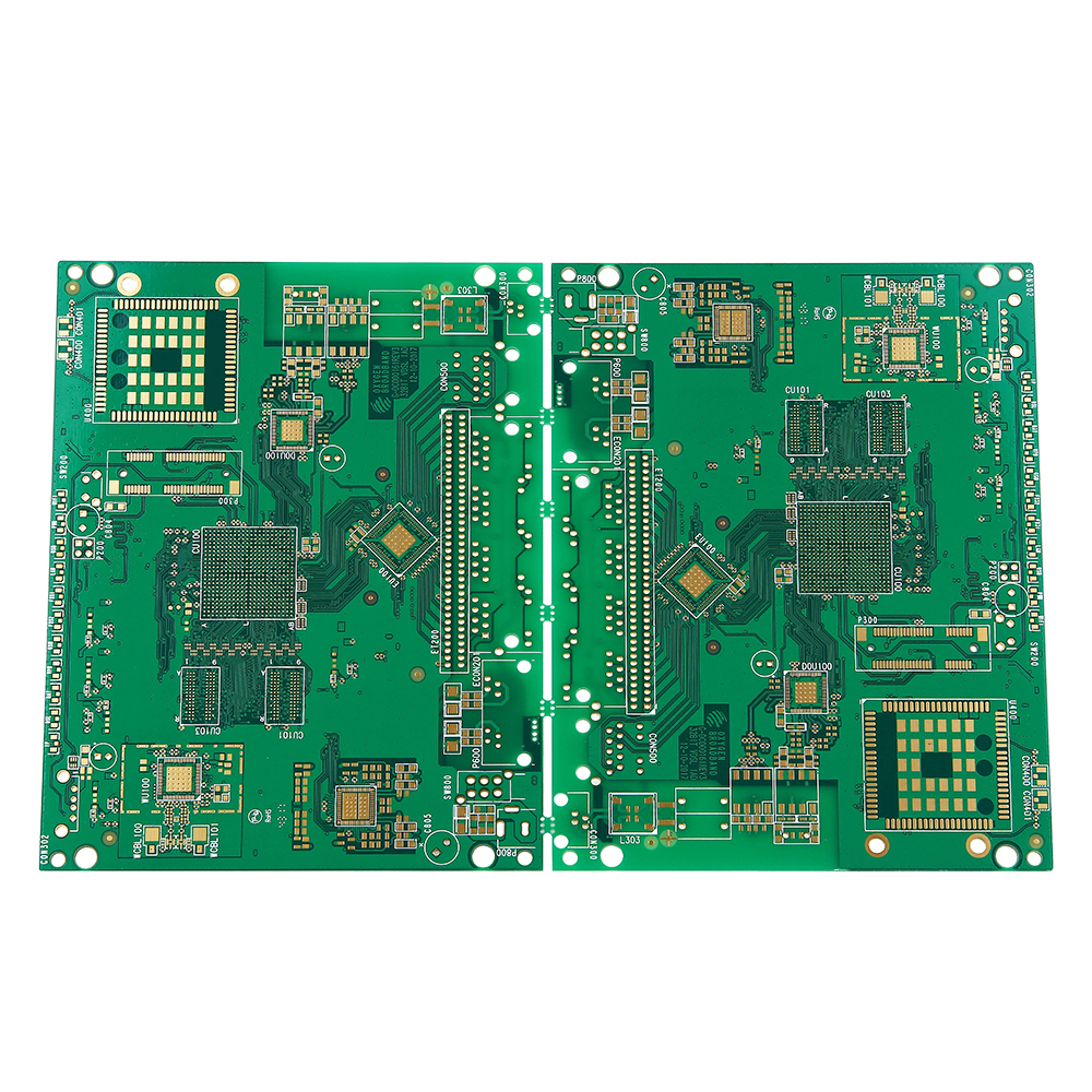
Multi-layer printed circuit boards (PCBs) are essential components in modern electronic devices, providing the foundation for complex and high-performance applications. This advanced design allows for greater circuitry density and enhanced electrical performance.
Key Features:
Increased Circuit Density: The stacked layers enable more complex and compact designs, accommodating advanced circuitry within a smaller footprint.
Enhanced Electrical Performance: Improved signal integrity and reduced electromagnetic interference (EMI) make multi-layer PCBs ideal for high-speed and high-frequency applications.
Thermal Management: Effective heat dissipation through the use of thermal vias and high-quality substrate materials ensures reliable operation of electronic components.
Versatility: Suitable for a wide range of applications, including telecommunications, medical devices, aerospace, automotive, and consumer electronics.
Material Options: Constructed using premium materials such as FR4, Rogers, and Teflon to meet specific electrical and thermal requirements.
Multi-layer PCBs provide a robust and reliable platform for sophisticated electronic systems, delivering the performance and functionality needed for today’s advanced technologies.
Quality Assurance Processes
Ensuring the highest quality and reliability of multi-layer PCBs is critical for their application in demanding environments. Our comprehensive quality assurance processes guarantee that every PCB meets stringent industry standards and exceeds customer expectations.
Quality Assurance Processes:
Design Verification:
DFM (Design for Manufacturability) Analysis: Thorough review of the PCB design to identify and correct potential manufacturing issues, ensuring optimal production efficiency and quality.
DFT (Design for Testability) Analysis: Evaluation of the PCB design to enhance testability, facilitating effective quality control and functional testing.
Material Inspection:
Incoming Material Quality Control: Rigorous inspection of raw materials, including copper, laminates, and solder masks, to ensure they meet specified quality standards before production.
Manufacturing Process Control:
Automated Optical Inspection (AOI): High-resolution AOI systems inspect each layer and assembled PCB for defects such as misalignment, solder bridges, and open circuits.
X-Ray Inspection: Advanced X-ray systems check for internal defects, including voids and misaligned layers, providing a thorough examination of the PCB’s structure.
Micro-Sectioning Analysis: Detailed examination of cross-sections of the PCB to assess layer alignment, via integrity, and plating quality.
Electrical Testing:
Flying Probe Testing: Non-contact testing of electrical connections to verify continuity and isolate defects without the need for test fixtures.
In-Circuit Testing (ICT): Comprehensive testing of individual components and circuits on the PCB to ensure they meet specified performance criteria.
Environmental and Reliability Testing:
Thermal Cycling: Exposure of the PCB to extreme temperature variations to ensure it can withstand thermal stress and operate reliably under different environmental conditions.
Humidity Testing: Evaluation of the PCB’s performance in high humidity environments to ensure long-term reliability and durability.
Vibration and Shock Testing: Assessment of the PCB’s mechanical robustness by subjecting it to vibration and shock conditions to simulate real-world usage.
Final Inspection and Functional Testing:
Visual Inspection: Final manual inspection to identify any cosmetic defects and ensure the PCB meets aesthetic standards.
Functional Testing: Simulation of real-world operating conditions to verify the PCB’s performance and functionality, ensuring it meets customer specifications.
Our dedication to rigorous quality assurance processes ensures that every multi-layer PCB we produce is of the highest quality, providing our customers with reliable, high-performance solutions for their advanced electronic applications.
 +86 755 2794 4155
  sales@knownpcb.com

 EN
EN CN
CN 中文
中文

 Home >