 +86 755 2794 4155
  sales@knownpcb.com
-
Shenzhen KNOWNPCB Technology Co., Ltd.
 +86 755 2794 4155
  sales@knownpcb.com
 2024-09-18
 658
658

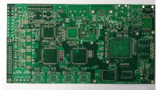
The PCB production process mainly includes steps such as design, graphic conversion, plate making, etching, drilling, coating, soldering, testing, and cleaning.
design phase
The design phase is the starting point of PCB production, where CAD software is used to design circuit schematics and PCB layouts, determining information such as PCB board dimensions, wiring methods, and pad sizes.
Graphic Conversion Stage
After the design is completed, it is necessary to convert the circuit schematic and PCB layout into Gerber files for plate making and etching processes.
Plate making stage
Plate making is the core process in PCB production, which involves converting Gerber files into photoresist film, and then transferring the photoresist film pattern onto copper foil through exposure, development, and other processes to create the circuit and graphics of the PCB board.
Etching stage
Etching is the process of removing unwanted copper foil parts by immersing the plated copper foil in an etchant, waiting for a certain period of time, and then etching off the excess copper foil to form the circuit and pattern of the PCB board.
Drilling stage
Drilling refers to drilling various holes on a PCB board, including pad holes, positioning holes, mounting holes, etc. Drilling requires the use of a drilling machine or drilling machine for operation.
Coating stage
Coating is the process of removing the photoresist film from the copper-clad laminate, and then covering it with a layer of solder film through drying, exposure, and other processes for subsequent welding operations.
Welding stage
Welding is the process of installing components onto a PCB board and performing welding. During the welding process, it is necessary to use a soldering iron or welding equipment for operation.
Testing phase
Testing is the process of quality inspection of PCB boards after welding, mainly including AOI testing, X-ray testing, ICT testing, etc.
Cleaning stage
Cleaning is the process of thoroughly cleaning the soldered PCB board for subsequent packaging and assembly operations.

Or call +86 755 2794 4155
Inquiry Now

