 +86 755 2794 4155
  sales@knownpcb.com
-
Shenzhen KNOWNPCB Technology Co., Ltd.
 +86 755 2794 4155
  sales@knownpcb.com
 2025-04-17
 167
167
PCB blistering is primarily caused by defects in the electroless copper plating and electroplating processes during circuit board manufacturing, representing one of the most prevalent quality issues. The root cause of board surface blistering fundamentally stems from poor adhesion (interfacial bonding failure) or surface quality defects on the copper-plated layer.
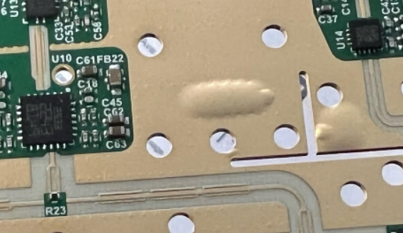
Key Causes of Blistering in Electroless Copper Plating and Electroplating:
• Improper Control of Micro-Etching in Pre-Treatment (Before Electroless Copper Plating and Pattern Plating):
Excessive micro corrosion can cause leakage of the substrate and foaming around the hole, while insufficient micro corrosion can lead to insufficient bonding force and foaming. It is necessary to strengthen micro corrosion control and pay attention to the copper content, bath temperature, load, and micro corrosion agent content of the micro corrosion groove.
• Excessive Activity of Electroless Copper Solution:
Freshly prepared baths or elevated copper content in key bath components (e.g., Cu²+) may cause overly aggressive deposition, resulting in rough copper surfaces, degraded plating quality, and poor adhesion.
Solutions: Reduce copper content, increase complexing agents/stabilizers, and lower bath temperature.
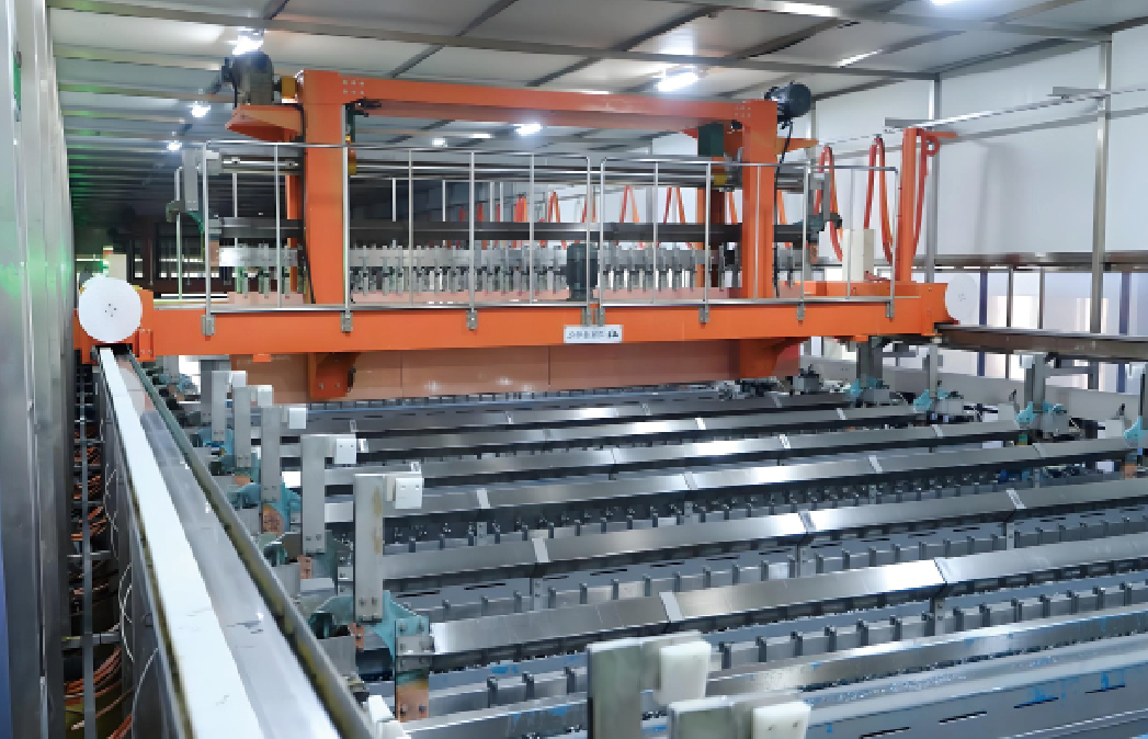
• Surface Oxidation During Production:
Oxidation of electroless copper layers in air can cause copper voids in through-holes, surface roughness, and blistering. Prolonged exposure to acidic environments forms stubborn oxide layers.
Recommendations: Minimize storage time; complete copper thickening (electroplating) within 12 hours post-electroless plating.
• Poor Rework Practices for Electroless Copper Layers:
Defects like incomplete stripping, improper rework methods, or incorrect micro-etching duration may induce blistering.Clean and acid-wash defective boards without micro-etching before reprocessing.
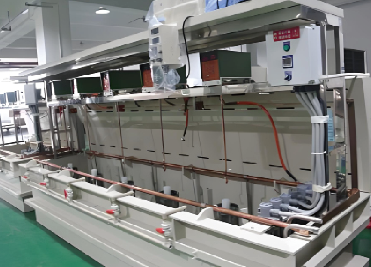
• Insufficient Rinsing Post-Developing in Pattern Transfer:
Extended post-developing delays or excessive workshop dust compromise surface cleanliness and fiberglass treatment, creating latent defects.
• Contaminated Acid Pre-Dip Tank Before Electroplating:
High contamination or copper content in the acid tank leads to p oor surface cleanliness and roughness.
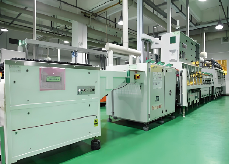
• Organic Contamination in Electroplating Baths:
Oil contamination (common in automated lines) significantly impacts plating quality.
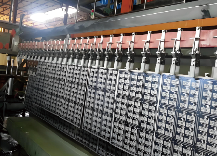
In the actual production of PCB boards, there are various reasons for surface blistering. Due to differences in equipment technology, the causes of blistering vary among different printed circuit board manufacturers and require specific analysis. This article provides a brief analysis of the production process flow, regardless of priority, aiming to provide problem-solving ideas and assist in process production and problem solving.

Or call +86 755 2794 4155
Inquiry Now

