 +86 755 2794 4155
  sales@knownpcb.com
-
Shenzhen KNOWNPCB Technology Co., Ltd.
 +86 755 2794 4155
  sales@knownpcb.com
 2025-01-10
 145
145

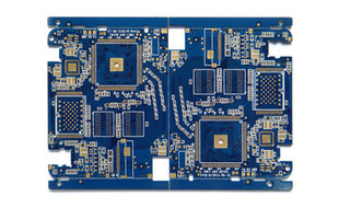
PCB layout is a critical step in the design of printed circuit boards. It involves arranging the electronic components on the board and routing the electrical connections between them. A well-designed PCB layout can improve the performance, reliability, and manufacturability of an electronic device.
The first step in PCB layout is to determine the placement of the major components. This includes the microcontroller, power supply, connectors, and other key components. The placement should be based on factors such as signal flow, power distribution, and thermal management.
Once the major components are placed, the smaller components can be added. These may include resistors, capacitors, diodes, and other discrete components. The placement of these components should be optimized to minimize the length of the traces and to reduce the risk of interference.
Routing the traces is the next step in PCB layout. The traces should be routed in a way that minimizes crosstalk and electromagnetic interference. This can be achieved by using ground planes, power planes, and shielding. The trace widths and spacings should also be optimized to ensure proper signal integrity.
In addition to routing the traces, the PCB layout should also include vias, which are used to connect different layers of the board. The placement and size of the vias should be carefully considered to ensure proper electrical connections and to minimize the risk of signal degradation.
Finally, the PCB layout should be checked for compliance with design rules and standards. This includes checking for proper clearance between components, trace widths and spacings, and via sizes. The layout should also be checked for manufacturability, ensuring that it can be fabricated using standard PCB manufacturing processes.
Overall, PCB layout is a complex and iterative process that requires a combination of electrical engineering knowledge, software skills, and practical experience. A well-designed PCB layout can greatly improve the performance and reliability of an electronic device.

Or call +86 755 2794 4155
Inquiry Now

