 +86 755 2794 4155
  sales@knownpcb.com
-
Shenzhen KNOWNPCB Technology Co., Ltd.
 +86 755 2794 4155
  sales@knownpcb.com
 2024-07-25
 656
656

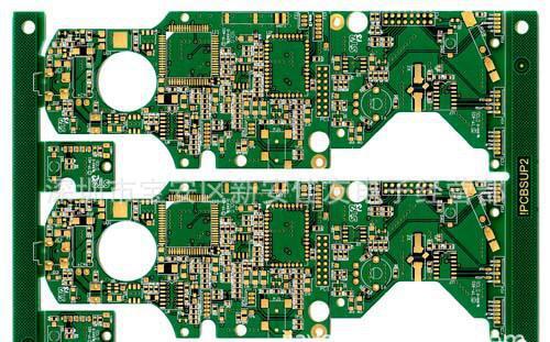
Ordinary printed circuit boards (PCBs) are an indispensable part of modern electronic devices. It forms complex circuit patterns by etching copper wires onto an insulating substrate, thereby connecting and supporting various electronic components. This type of circuit board typically consists of several layers, including a top layer, a bottom layer, and an inner layer. The more layers there are, the more complex the functions of the circuit board become, and the corresponding cost increases.
When designing a regular printed circuit board, engineers need to consider multiple factors such as circuit layout, signal integrity, power management, etc. The circuit layout determines the arrangement of components and the direction of wires, directly affecting the performance and reliability of the circuit. Signal integrity refers to the degree to which a signal maintains its original shape during transmission, which is particularly important for high-speed circuits. Power management involves how to effectively allocate and manage electrical energy to ensure stable circuit operation.
The process of manufacturing ordinary printed circuit boards includes steps such as plate making, exposure, development, etching, drilling, and assembly. Firstly, the circuit pattern is transferred onto the copper-clad laminate using photolithography technology. Then, the pattern is solidified on the board through exposure and development processes. Next, use chemical etching to remove unwanted copper foil and form the final circuit pattern. The drilling process is used to install interlayer connections between components and multi-layer boards. Finally, solder various electronic components onto the circuit board to complete the assembly.
Ordinary printed circuit boards are widely used in fields such as household appliances, computers, and communication equipment. Their low cost and high reliability make them the preferred choice for electronic product manufacturing.

Or call +86 755 2794 4155
Inquiry Now

