 +86 755 2794 4155
  sales@knownpcb.com
-
Shenzhen KNOWNPCB Technology Co., Ltd.
 +86 755 2794 4155
  sales@knownpcb.com
 2024-07-27
 815
815

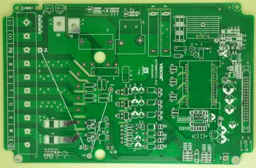
The Main PCB is the core component in electronic devices, carrying the main electronic components and circuits. It is usually located at the center of the device and communicates with other sub circuit boards or modules through connectors. The design and layout of the main PCB directly affect the performance and reliability of the entire system.
When designing the main PCB, engineers need to consider multiple factors comprehensively, including circuit layout, signal integrity, power distribution, thermal management, and mechanical structure. Reasonable layout can reduce signal interference and energy loss, improve system stability and efficiency. The design of the power distribution network is also crucial to ensure stable power supply to all parts.
The main PCB usually adopts a multi-layer structure to facilitate complex wiring and functional zoning. Common layers include 4, 6, 8, etc. Each layer is connected through through holes and vias to achieve electrical connections and signal transmission. In order to enhance the reliability and durability of circuit boards, the main PCB is often subjected to surface treatments such as tin plating, gold plating, or OSP (organic solder paste) treatment.

Or call +86 755 2794 4155
Inquiry Now

