 +86 755 2794 4155
  sales@knownpcb.com
-
Shenzhen KNOWNPCB Technology Co., Ltd.
 +86 755 2794 4155
  sales@knownpcb.com


Key Features and Benefits
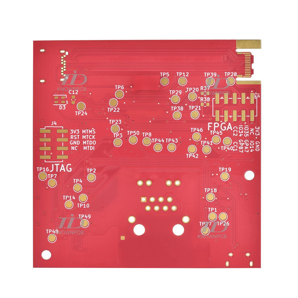
Our 2 double-layer PCBs are designed to provide superior performance, reliability, and flexibility for various applications. These PCBs are ideal for more complex designs that require additional layers to accommodate intricate circuitry and high component density.
Key Features:
Double-Layer Construction: Utilizing two layers of copper, these PCBs offer enhanced routing options, allowing for more complex and compact designs.
Versatile Applications: Suitable for a wide range of applications, including consumer electronics, automotive, medical devices, industrial control systems, and telecommunications.
Improved Performance: The additional layer provides increased electrical performance and reliability, reducing the risk of signal loss and interference.
Efficient Space Utilization: Maximizes the use of available space, enabling more components to be placed on the PCB without increasing its size, ideal for compact and portable devices.
Benefits:
Enhanced Design Flexibility: The double-layer design allows for more intricate and efficient circuit layouts, accommodating complex projects and reducing PCB size.
Improved Electrical Performance: High-quality materials and precise manufacturing ensure reliable and high-performance PCBs, meeting the needs of demanding applications.
Power Integrity
Power integrity is crucial for the performance and reliability of electronic systems. Our 2 double-layer PCBs are designed with features that enhance power integrity, ensuring stable and reliable power delivery throughout the board.
Power Integrity Details:
Dedicated Power and Ground Planes: The use of dedicated power and ground planes helps to reduce noise, providing a stable reference for signal traces and improving overall power distribution.
Low Impedance Power Delivery: Careful design and placement of power and ground planes ensure low impedance paths, minimizing voltage drops and ensuring efficient power delivery to all components.
Decoupling Capacitors: Strategically placed decoupling capacitors near power pins help to filter out noise and provide a stable power supply to critical components.
Controlled Impedance: Ensures consistent and predictable power distribution, reducing the risk of power-related issues in high-speed and high-frequency applications.
Minimized Power Noise: Design techniques such as proper trace width and spacing, as well as the use of power planes, help to minimize power noise and maintain signal integrity.
Thermal Management: Effective thermal management solutions help to dissipate heat, maintaining stable power performance even under high-power conditions.
EMI/RFI Mitigation: Design strategies to reduce electromagnetic interference (EMI) and radio frequency interference (RFI), maintaining the integrity of power and signal lines.
Robust Via Design: Proper via design and placement reduce parasitic inductance and capacitance, further enhancing power integrity and ensuring reliable connections between layers.
Surface Finish Options: Various surface finishes, such as HASL (Hot Air Solder Leveling), ENIG (Electroless Nickel Immersion Gold), and OSP (Organic Solderability Preservatives), are available to ensure optimal power performance and reliability.
By focusing on power integrity, our 2 double-layer PCBs ensure that your electronic designs operate reliably and efficiently. Our commitment to quality and precision manufacturing guarantees that your projects will benefit from stable and robust power delivery, meeting the high standards required for modern electronic applications. Contact us today to learn more about how our double-layer PCB solutions can enhance your electronic designs.
Inquiry Now

