 +86 755 2794 4155
  sales@knownpcb.com
-
Shenzhen KNOWNPCB Technology Co., Ltd.
 +86 755 2794 4155
  sales@knownpcb.com
 2024-07-10
 455
455

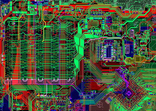
Copper circuit boards mainly consist of the following parts:
1. Substrate: usually fiberglass cloth impregnated with epoxy resin or other synthetic resins to form a hard composite material.
2. Copper foil: A thin layer of copper covering the surface of the substrate, typically ranging in thickness from a few micrometers to tens of micrometers.
3. Circuit pattern: A conductive path formed on copper foil through processes such as etching and electroplating, used to connect various electronic components.
The process of manufacturing copper circuit boards mainly includes the following steps:
1. Design and plate making: Use computer-aided design (CAD) software to design circuit patterns and create photo plates.
2. Lamination: The copper foil and substrate are bonded together by hot pressing.
3. Exposure and development: Use photosensitive resin and photoresist to expose and develop, forming a mask for circuit patterns.
4. Etching: By chemical etching or laser cutting, unwanted copper foil is removed to form the final circuit pattern.
5. Drilling and Coating: Drill necessary installation holes and through holes on the circuit board, and apply copper plating treatment to enhance conductivity and corrosion resistance.
6. Surface treatment: Apply tin lead coating, OSP (organic solder flux) treatment, or other surface treatment processes to protect the circuit board and improve soldering performance.

Or call +86 755 2794 4155
Inquiry Now

