 +86 755 2794 4155
  sales@knownpcb.com
-
Shenzhen KNOWNPCB Technology Co., Ltd.
 +86 755 2794 4155
  sales@knownpcb.com
 2023-08-15
 480
480

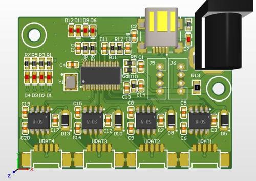
As the name suggests, a multi-layer circuit board can only be called a multi-layer circuit board if it has two or more layers. Previously, we analyzed what a double-sided circuit board is, so a multi-layer board is more than two layers, such as four layers, six layers, eight layers, and so on. Of course, some designs are three or five layer circuits, also known as multi-layer PCB circuit boards. A conductive wiring diagram larger than a two-layer board, with insulating substrates separating the layers. After each layer of wiring is printed, it is then pressed together to overlap each layer of wiring. Afterwards, drilling will be carried out to achieve continuity between each layer of the line through holes. The advantage of multi-layer PCB circuit boards is that the circuits can be distributed and wired within multiple layers, allowing for the design of more precise products. Or smaller products can be achieved through multi-layer boards. Products with larger volumes such as mobile phone circuit boards, mini projectors, and recording pens. In addition, multiple layers can increase design flexibility, allowing for better control of differential impedance and single ended impedance, as well as better output of some signal frequencies
Multilayer circuit boards are an inevitable product of the development of electronic technology towards high speed, multifunctional, large capacity, and small volume. With the continuous development of electronic technology, especially the widespread and in-depth application of large-scale and ultra large scale integrated circuits, multi-layer printed circuits are rapidly developing towards high-density, high-precision, and high-level digitization, and technologies such as fine lines, small aperture penetration, blind hole buried holes, and high plate thickness to aperture ratio have been proposed to meet the needs of the market. Due to the need for high-speed circuits in the computer and aerospace industries, which require further improvement in packaging density, coupled with the reduction in size of separated components and the rapid development of microelectronics, electronic devices are developing towards a direction of volume reduction and mass reduction; Due to the limitations of available space, it is no longer possible to achieve further improvement in assembly density for single and double-sided printed boards. Therefore, it is necessary to consider using printed circuits with more layers than double-sided boards. This creates conditions for the emergence of multi-layer circuit boards.

Or call +86 755 2794 4155
Inquiry Now

