 +86 755 2794 4155
  sales@knownpcb.com
-
Shenzhen KNOWNPCB Technology Co., Ltd.
 +86 755 2794 4155
  sales@knownpcb.com
 2023-11-15
 281
281

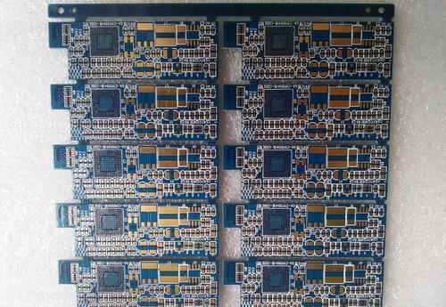
The so-called PCB sampling actually refers to the trial production of printed circuit boards before mass production, which is the process of electronic engineers designing circuits and completing PCBs, and PCB manufacturers conducting small-scale trial production. After the sample testing is completed, mass production will be carried out. There are two methods for sampling, one is a legitimate PCB factory, and the other is a professional sampling company. PCB sampling generally includes two groups, one is the engineer group, and the other is the PCB sampling manufacturer.
As a team of engineers, attention should be paid to the following aspects when making samples: 1. Only by carefully selecting the sample size can we effectively control costs. 2. Confirm the packaging of the equipment to avoid packaging errors that may lead to sample failure. 3. Conduct comprehensive electrical testing to improve the electrical performance of the PCB board. 4. Complete signal integrity layout, reducing noise, and improving PCB stability. As a PCB sampling manufacturer, attention should be paid to: 1. Carefully check the PCB document to avoid data issues. 2. Conduct comprehensive process approval and configuration with your own manufacturer. 3. Control production quantity, reduce costs, and ensure quality. 4. Communicate with customers on sampling precautions and prevent accidents and unnecessary losses in advance. The layout and wiring of components have a significant impact on the product's service life, stability, and electromagnetic compatibility, and special attention should be paid. Pay attention to the placement order of the components. Usually, fixed components related to the structure are placed first, while other components are placed in descending order. In addition, the component layout also needs to pay attention to heat dissipation issues, and the heating elements should be placed separately, not concentrated in one place. After the PCB wiring is completed, some adjustments need to be made to the application of text, individual components, wiring, and copper for production, debugging, and maintenance. 3. Use the simulation function to ensure that the PCB can be correctly sampled, and software simulation can be used. Especially for high-frequency digital circuits, some problems can be identified in advance, reducing the workload of later debugging.

Or call +86 755 2794 4155
Inquiry Now

