 +86 755 2794 4155
  sales@knownpcb.com
-
Shenzhen KNOWNPCB Technology Co., Ltd.
 +86 755 2794 4155
  sales@knownpcb.com
 2023-10-13
 161
161

With the development of technology, some high-tech devices are becoming increasingly miniaturized and precise, which puts higher demands on the HDI boards they use.
The line width/spacing of HDI circuit boards for some devices has evolved from early 0.13 mm (5 mils) to 0.075 mm (3 mils) and has become a mainstream standard. As a leading enterprise in the HDI fast board industry, Shenzhen Benqiang Circuit Co., Ltd. has achieved a production process of 38 μ M (1.5 mil) is approaching the limit of the industry.
The increasingly high requirements for line width/distance have brought the most direct challenge to graphic imaging in the PCB manufacturing process. So how are the copper wires on these precision boards processed and formed?
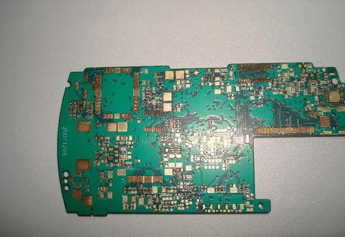
The important feature of HDI circuit boards is the presence of micro through holes (aperture ≤ 0.10 mm), all of which belong to buried blind hole structures.
The buried blind holes on HDI boards are currently mainly processed by laser, but there are also CNC drilling.
Compared to laser drilling, mechanical drilling also has its own advantages. When laser processing epoxy glass cloth dielectric layer through holes, the difference in ablation rate between the glass fiber and the surrounding resin can lead to slightly poor quality of the holes, and residual glass fiber fibers on the hole wall can affect the reliability of the through holes. Therefore, the superiority of mechanical drilling is reflected at this time. In order to improve the reliability and drilling efficiency of PCB boards, laser drilling and mechanical drilling technologies are steadily improving.

Or call +86 755 2794 4155
Inquiry Now

