 +86 755 2794 4155
  sales@knownpcb.com
-
Shenzhen KNOWNPCB Technology Co., Ltd.
 +86 755 2794 4155
  sales@knownpcb.com
 2024-01-10
 545
545

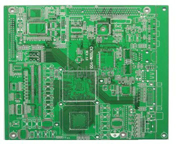
In order to save production costs, almost every PCB factory performs panel assembly operations before orders enter the workshop. Splicing boards is not just about putting various small boards together into one big board, but there are many things to pay attention to and important principles. Today, let the editor of Zhongxinhua summarize with everyone~
Firstly, there is the issue of splicing, and the reason for this is to save production costs. To avoid unnecessary waste, splicing treatment will be carried out before production on the circuit board production line without affecting the circuit board.
For PCB panel width ≤ 260mm~300mm, it varies depending on the production line. Because we may have many materials and each material gun corresponds to a module in our own processing equipment, if the splicing exceeds the range of the module, the processing speed will become very slow.
The outer frame (clamping edge) of the PCB panel should be carefully considered to ensure that the PCB panel will not deform after being fixed on the fixture (V-grooves are generally not allowed on this edge). For the layout of components, the orientation of all components should be consistent and there should be no mirror image, which may cause coordinate positioning problems in processing.
Secondly, there should be no connector extension at the edges (between the outer frame of the panel and the inner small board, or between the small board and the small board). If this situation exists, it will hinder the tool from dividing the board after welding is completed.
In order to ensure the position and level of the detection board, we need to set more than three positioning points on the edge of the board. Through optical detection of these three points, the reference coordinates of the entire processing and the levelness of the board can be obtained.

Or call +86 755 2794 4155
Inquiry Now

