 +86 755 2794 4155
  sales@knownpcb.com
-
Shenzhen KNOWNPCB Technology Co., Ltd.
 +86 755 2794 4155
  sales@knownpcb.com
 2023-05-23
 227
227

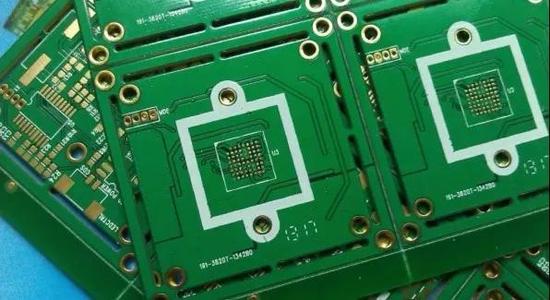
1. Scan the upper and lower surfaces of the circuit board, there are two BMP pictures.
2. Open the copy software QuickPCB2005, click "File" and "Open the bottom diagram" to open a scanning picture. Use Pageup to amplify the screen, see the pad, place a pad in PP, see the line and press PT to walk ... Just like a child drawing, draw it in this software, click "Save" to generate a B2P file.
3. Click the "File" and "Open the bottom diagram" to open another layer of scanning color map;
4. Click the "File" and "Open" to open the B2P file saved in front. We see the just copied board and stacked on this picture -the same PCB board, the hole is in the same position, but the line connection is different from different line connections. Essence Therefore, we according to the "Options" - "layer settings", here to turn off the displayed lines and silk prints, leaving only a multi -layer perforated.
5. The excessive hole on the top layer is in the same position as the perforated on the bottom picture, and then the bottom line is sufficient like a childhood drawing. Click "Save" again -at this time the B2P file has the top and bottom layer information.
6. Click "File" and "Export as a PCB file" to get a PCB file with two layers of information. You can change the board or send a schematic diagram or directly send the PCB mode of production

Or call +86 755 2794 4155
Inquiry Now

