 +86 755 2794 4155
  sales@knownpcb.com
-
Shenzhen KNOWNPCB Technology Co., Ltd.
 +86 755 2794 4155
  sales@knownpcb.com
 2024-06-25
 155
155

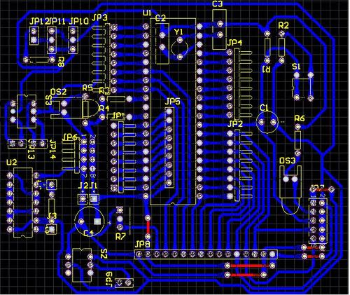
Copper coating refers to using the idle space on the PCB as a reference plane and then filling it with solid copper. These copper areas are also known as copper filling. The significance of copper plating is to reduce the impedance of the ground wire and improve its anti-interference ability; Reduce voltage drop and improve power efficiency; Also, connect to the ground wire to reduce the loop area. If there is a lot of ground on a PCB, such as SGND, AGND, GND, etc., how to cover it with copper? My approach is to use the most important "ground" as a reference for independent copper plating based on the different positions of the PCB board, and to separate the digital and analog copper plating without much explanation. Before copper plating, first thicken the corresponding power lines: V5.0V, V3.6V, V3.3V (SD card power supply), and so on. In this way, multiple deformation structures with different shapes are formed.
There are several issues that need to be addressed in copper plating: first, single point connections at different locations; second, copper plating near the crystal oscillator. The crystal oscillator in the circuit serves as a high-frequency emission source. The method is to lay copper around the crystal oscillator and then ground the outer shell of the crystal oscillator separately. The third issue is the problem of isolated islands (dead zones). If you feel it is very large, then defining a ground through hole and adding it doesn't require much effort.
Furthermore, it is not easy to generalize whether it is better to cover a large area with copper or to cover the grid with copper. Why? Large area copper coating may cause the board to curl up and even bubble during wave soldering. From this perspective, the heat dissipation of the grid is better. Usually, it is a multi-purpose grid with high anti-interference requirements for high-frequency circuits, and a complete copper laying is commonly used for circuits with high current in low-frequency circuits.

Or call +86 755 2794 4155
Inquiry Now

