 +86 755 2794 4155
  sales@knownpcb.com
-
Shenzhen KNOWNPCB Technology Co., Ltd.
 +86 755 2794 4155
  sales@knownpcb.com
 2023-12-21
 917
917

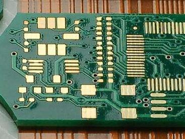
① Inner layer production: Multilayer circuit boards are made by pressing two or more double-sided boards. For some high-frequency multi-layer boards, the inner layer holes may be blind holes, and the inner layer boards need to be drilled and then pressed together.
② Drilling: Based on the production capacity of the factory, verify the data. If the line width moment or aperture is less than the manufacturing capacity, the engineering department should improve communication with the customer and reach a consensus to compensate for a certain stroke of the line width moment or aperture. Generally, the drilling roughness is controlled at ≤ 25.4um.
③ Copper plating: Usually, during transportation or production, there may be scratches on the substrate copper foil, causing it to be exposed to the surface. It is necessary to go through processes such as copper plating to ensure that the thickness of the PCB board copper foil meets the customer's order requirements. Secondly, according to the MI copper thickness requirements, suitable current parameters should be selected for the current group.
④ Electroplating nickel gold/etching: Follow the strict requirements of the MI process to perform routine electroplating current indication operations. Before etching the circuit board, priority should be given to using 3M tape for tensile testing. If any defects are found, stop immediately and inform the on duty supervisor or supervisor.
⑤ Solder resistance: When printing solder resistance ink, first understand whether the customer requires through-hole cover oil or through-hole window opening. The technical personnel who make the film need to carefully review this note. Solder resistance through-hole cover oil refers to the copper inside the hole being covered by the ink, while through-hole window opening refers to the copper inside the hole not being covered.
⑥ Surface treatment: Different surface treatment processes also have different processing times. Tin spraying/OSP is faster, while gold deposition/plating is slower. Secondly, it is best not to pick up the circuit board directly by hand to avoid oxidation.

Or call +86 755 2794 4155
Inquiry Now

